Integrated circuit memory devices having automatically induced standby modes and methods of operating same

a technology of integrated circuit memory and standby mode, which is applied in the direction of information storage, static storage, digital storage, etc., can solve the problems of power consumption requirements

Inactive Publication Date: 2000-08-08
SAMSUNG ELECTRONICS CO LTD
View PDF3 Cites 29 Cited by
  • Summary
  • Abstract
  • Description
  • Claims
  • Application Information

AI Technical Summary

Problems solved by technology

However, because devices such as TTL buffers may remain active in SDRAMs whenever a clock enable signal (CKE) is active, even if the buffers are not actively buffering data, there is a continuing need to develop additional techniques to reduce power consumption requirements in devices which may be battered powered.

Method used


Image

  • Integrated circuit memory devices having automatically induced standby modes and methods of operating same
  • Integrated circuit memory devices having automatically induced standby modes and methods of operating same
  • Integrated circuit memory devices having automatically induced standby modes and methods of operating same

Examples


Embodiment Construction

The present invention will now be described more fully hereinafter with reference to the accompanying drawings, in which preferred embodiments of the invention are shown. This invention may, however, be embodied in different forms and should not be construed as limited to the embodiments set forth herein. Rather, these embodiments are provided so that this disclosure will be thorough and complete, and will fully convey the scope of the invention to those skilled in the art. Like numbers refer to like elements throughout and signal lines and signals thereon may be referred to by the same reference symbols.

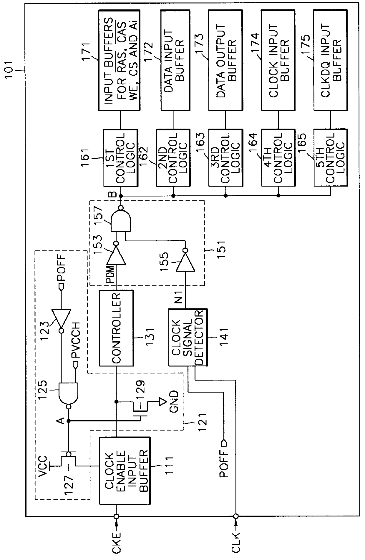
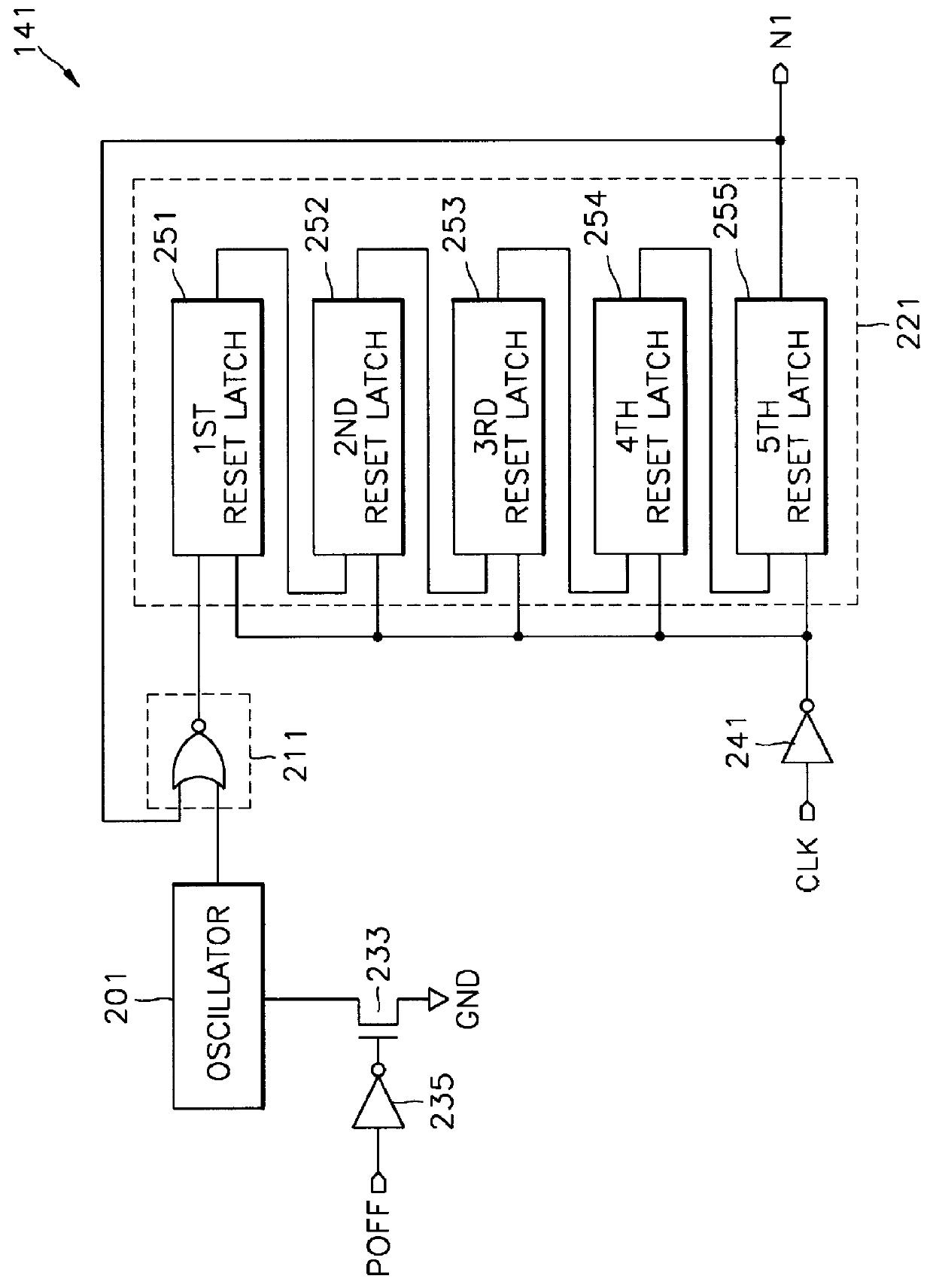
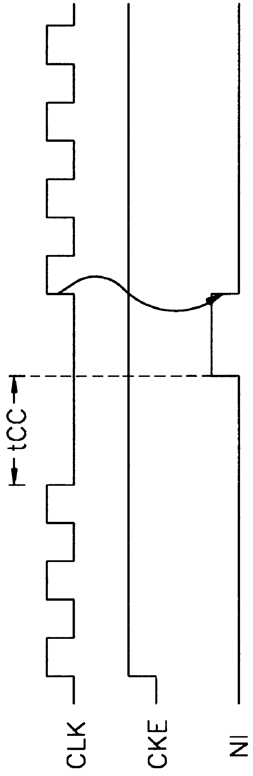
Referring now to FIG. 1, a preferred integrated circuit memory device 101 (e.g., SDRAM) according to an embodiment of the present invention is illustrated. This memory device includes a clock enable input buffer 111 which receives a clock enable signal CKE (e.g., at a TTL voltage level) and passes this clock enable signal CKE to a controller 131 (e.g., at a CMOS voltage level) when ...


PUM


Abstract

Integrated circuit memory devices monitor clock signal transitions and automatically induce a power saving standby mode of operation if the clock signal becomes inactive for a designated amount of time. The memory devices include at least one buffer having an active mode and an inactive standby mode and a standby current control circuit. This control circuit disposes the at least one buffer in its inactive standby mode whenever a power down signal is in a first logic state or whenever the power down signal is in a second logic state at a point in time when a clock signal has continuously been in an inactive state for a duration greater than twice its period. The control circuit may comprise a clock signal detector having N serially-connected latches therein which are reset whenever the clock signal transitions from the inactive state to an active state. The clock signal detector is responsive to the power down signal and comprises an oscillator which is active whenever the power down signal is in the second logic state and inactive whenever the power down signal is in the first logic state.

Description

This application is related to Korean Application No. 98-18827, filed May 25, 1998, the disclosure of which is hereby incorporated herein by reference.1. Field of the InventionThe present invention relates to integrated circuit devices, and more particularly to integrated circuit memory devices and methods of operating integrated circuit memory devices.2. Background of the InventionNotwithstanding recent advances in developing more highly integrated semiconductor devices, the increasing use of battery powered computer and communication systems has required the development of devices having substantially reduced power consumption requirements. To reduce the power consumption requirements of synchronous DRAM devices (which may contain TTL buffers having relatively high current requirements when active), power down signals have been utilized to induce a power saving standby mode during time periods when one or more devices need not be active. However, because devices such as TTL buffer...

Claims


Application Information

Patent Timeline
Patent Type & Authority Patents(United States)
IPC IPC(8): G11C7/22G11C7/00G11C11/409G11C11/401G11C11/407
CPCG11C7/22G11C11/401
Inventor JO, SEONG-KUE
Owner SAMSUNG ELECTRONICS CO LTD
Why Eureka
Try Eureka