Power MOSFET having laterally three-layered structure formed among element isolation regions

a technology of mosfet and element isolation, which is applied in the direction of semiconductor devices, electrical equipment, transistors, etc., can solve the problems of cost and time, complicated manufacturing process of mosfet disclosed in document 1 and difficulty in meeting both conditions

Inactive Publication Date: 2002-06-25
KK TOSHIBA
View PDF13 Cites 232 Cited by
  • Summary
  • Abstract
  • Description
  • Claims
  • Application Information

AI Technical Summary

Problems solved by technology

Such opposite relation exists, and it is difficult to satisfy both conditions.
Additionally, a manufacturing process of the MOSFET disclosed in Document 1 is complicated, because epitaxial growth of silicon, patterning, and ion implantation need to be repeated a plurality of times (six times in FIG. 1).
With such very long process, cost and time are required.
It is feared that a manufacturing cost largely rises.
However, also in this method, two ion implantation steps are necessary for forming the N and P pillar layers for one element of MOSFET, and further there is a restriction that only a MOSFET having a stripe pattern as a planar form can be formed.

Method used


Image

  • Power MOSFET having laterally three-layered structure formed among element isolation regions
  • Power MOSFET having laterally three-layered structure formed among element isolation regions
  • Power MOSFET having laterally three-layered structure formed among element isolation regions

Examples


Embodiment Construction

>

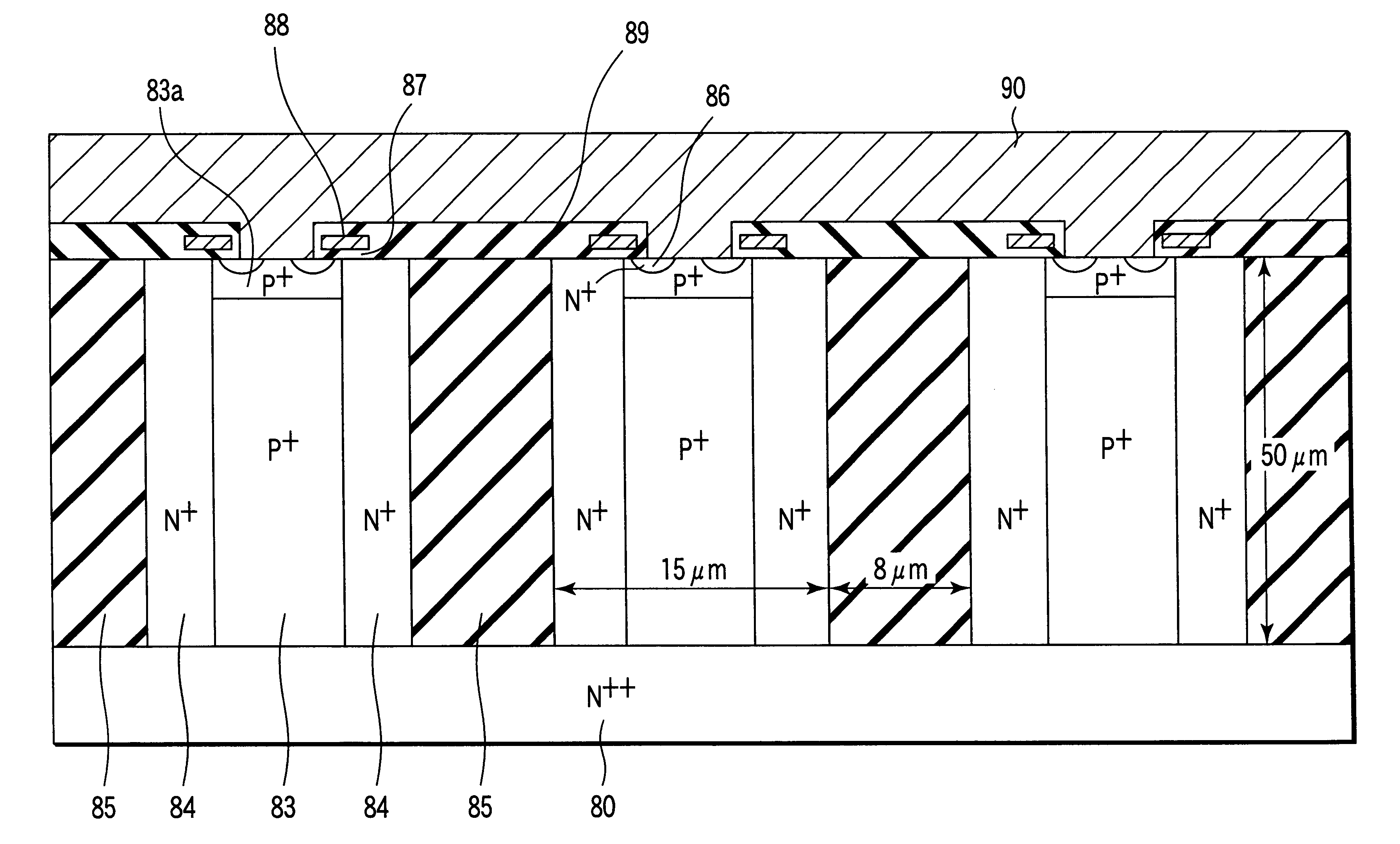
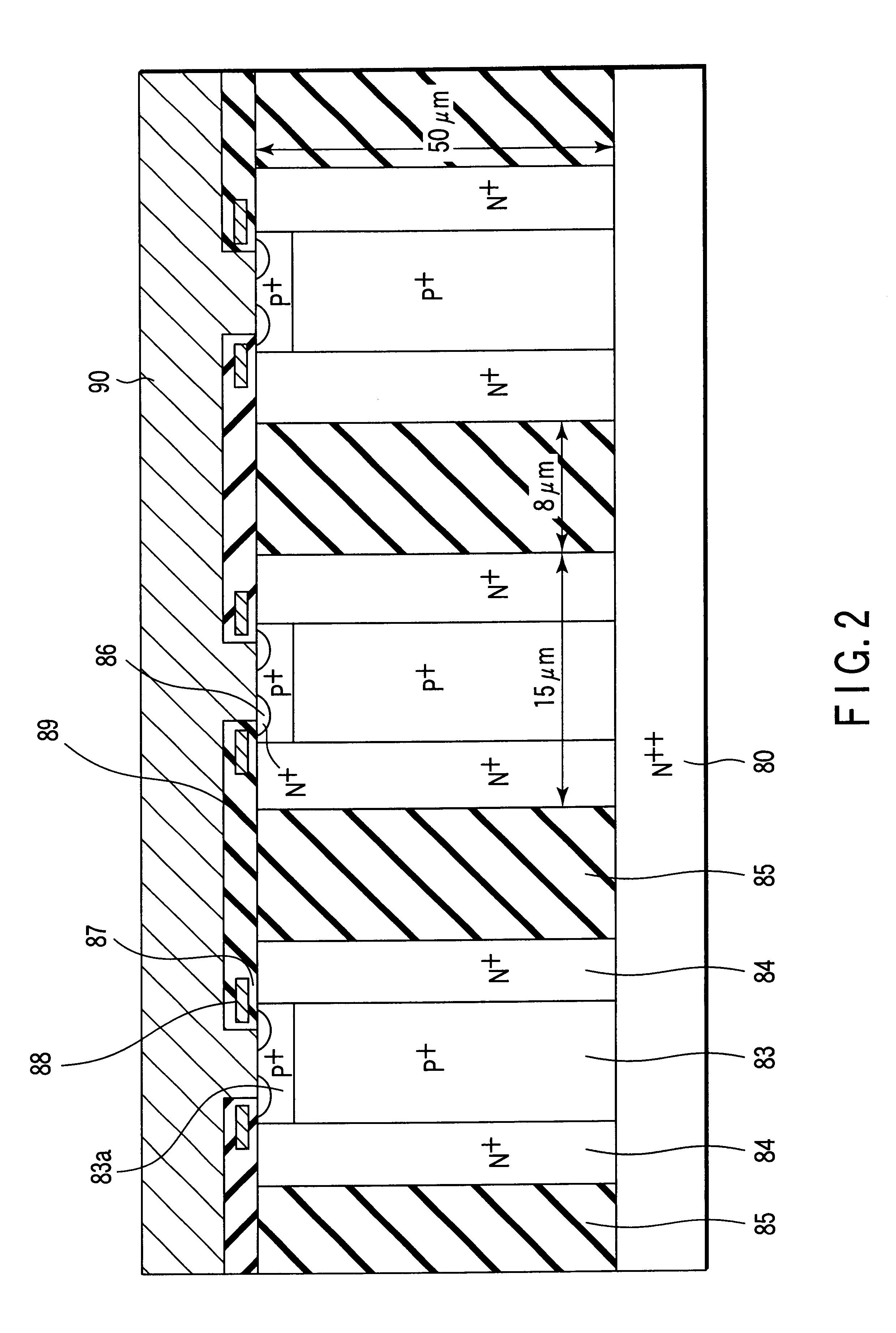
In the first to third embodiments, as shown in FIG. 5, the N.sup.++ region 84a may be formed in the portion continued to the trench side wall portion in the surface of the N.sup.+ pillar layer 13, so that the depletion layer is prevented from reaching the upper surface of the N.sup.+ pillar layer 13 during applying of the voltage.

Moreover, for the element isolation region and edge termination isolation region, as shown in FIG. 6, after formation of the dielectric film (e.g., Si.sub.3 N.sub.4 or SiO.sub.2) 85a on the trench inner wall, the insulator (poly silicon or SiO.sub.2) 85b may be buried.

Additionally, in the above description, the N-type DTMOS has been described, but the present invention can similarly be applied to a P-type DTMOS. In this case, a first conductivity type is a p-type, a second conductivity type is an n-type, and the P.sup.+ pillar layer in a PNP pillar layer constitutes the current path between the P.sup.+ source region and the drain.

Additional advantages and ...


PUM


Abstract

A semiconductor apparatus has an NPN (or PNP) laterally three-layered pillar formed in a mesh form among a plurality of trench type element isolation regions, and having a source and gate on an upper surface of the three-layered pillar, and a drain on a lower surface thereof. A depth DT and minimum planar width WTmin of the element isolation region and a width WP of the three-layered pillar are configured to satisfy a relation of 3.75<=DT / WP<=60 or 5.5<=DT / WTmin<=14.3. The above configuration realizes a high breakdown voltage and low on-resistance are realized.

Description

This application is based upon and claims the benefit of priority from the prior Japanese Patent Application No. 2000-359762, filed Nov. 27, 2000, the entire contents of which are incorporated herein by reference.1. Field of the InventionThe present invention relates to a semiconductor apparatus, particularly to a semiconductor apparatus in which a MOSFET is formed on an Si pillar of a longitudinal and laterally three-layered structure of NPN (or PNP), and to a structure suitable for a power switching device which requires a low on-resistance / high breakdown voltage.2. Description of the Related ArtA power switching device utilizing a MOSFET is required to have a low on-resistance / high breakdown voltage. In a power MOSFET having a conventional planar structure, however, when the on-resistance is lowered, the breakdown voltage is also lowered. When the breakdown voltage is raised, the on-resistance is raised. The device has an opposite relation.That is, in the power MOSFET of the plan...

Claims


Application Information

Patent Timeline
Patent Type & Authority Patents(United States)
IPC IPC(8): H01L29/78H01L29/66H01L29/02H01L29/06H01L21/336H01L21/76
CPCH01L29/0634H01L29/7802H01L29/0696H01L29/0653H01L29/7811H01L29/78
Inventor USUI, YASUNORIKOUZUKI, SHIGEO
Owner KK TOSHIBA
Why Eureka
Try Eureka