SRAM bus architecture and interconnect to an FPGA

a sram bus and interconnection technology, applied in pulse techniques, instruments, peptide sources, etc., can solve the problems of undesirable fpga design, less than satisfactory solutions, and insufficient memory provisioning by having other than explicitly dedicated sram blocks included in the fpga

Inactive Publication Date: 2002-12-17
ACTEL CORP
View PDF2 Cites 117 Cited by
  • Summary
  • Abstract
  • Description
  • Claims
  • Application Information

AI Technical Summary

Problems solved by technology

However, providing this memory by having other than explicitly dedicated SRAM blocks included in the FPGA has not proved satisfactory.
Both of these solutions are less than satisfactory.
Using external SRAMs with FPGA designs is undesirable for several reasons.
Separate memory chips are expensive, require additional printed circuit board space, and consume I / O pins on the FPGA itself.
Also, a separate memory chip is required to implement each memory function, thereby further increasing the cost.
This substantially degrades both the performance and flexibility of the FPGA by consuming a considerable amount of logic array resources, and imposes critical paths that are quite long for even a small memory block.
While this distributed SRAM approach is an improvement in density and is flexible for building larger memories, it is still slow and consumes logic array resources.
On their 4000-E Series parts, they offer the ability to configure two configurable logic blocks to emulate a dual ported 16.times.1 SRAM block, however, this design still carries with it performance and flexibility degradation.
This approach builds the flexibility of different widths and depths into the SRAM block, but at a significant performance cost since the access time of an embedded array block is very slow for a memory of the size and the technology in which it is built.
However, the local interconnect structure disclosed in Wilton suffers performance problems due to excessive flexibility in the interconnect architecture.
Unfortunately, this approach required array routing resources to interconnect SRAM blocks into deeper and wider configurations.
The difficulty in creating deeper and wider SRAM block configurations in the prior art has been that array routing resources have been required to interconnect the SRAM blocks into these configurations.
Part of the problem has been that the array routing resources have not been used very efficiently.

Method used


Image

  • SRAM bus architecture and interconnect to an FPGA
  • SRAM bus architecture and interconnect to an FPGA
  • SRAM bus architecture and interconnect to an FPGA

Examples


Embodiment Construction

Those of ordinary skill in the art will realize that the following description of the present invention is illustrative only and not in any way limiting. Other embodiments of the invention will readily suggest themselves to such skilled persons.

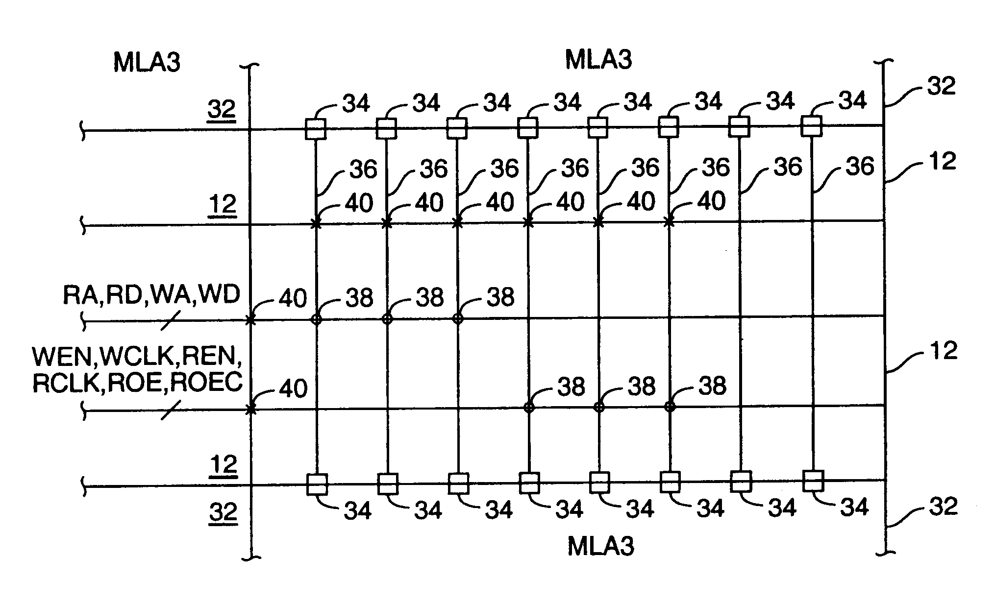
In the present invention, the SRAM bus architecture associated with the SRAM blocks is distinct from the general interconnect architecture of the FPGA. As will be described below, a distinct SRAM bus architecture provides advantages in connecting the SRAM blocks to the other portions of the FPGA not contemplated by the prior art. The SRAM bus architecture of the present invention does not require the use of the routing resources of the general interconnect architecture of the FPGA to connect SRAM blocks together in the manner known in the prior art, and can make use of the overhead generally allocated in SRAM blocks for the formation of address busses, data busses, and control lines.

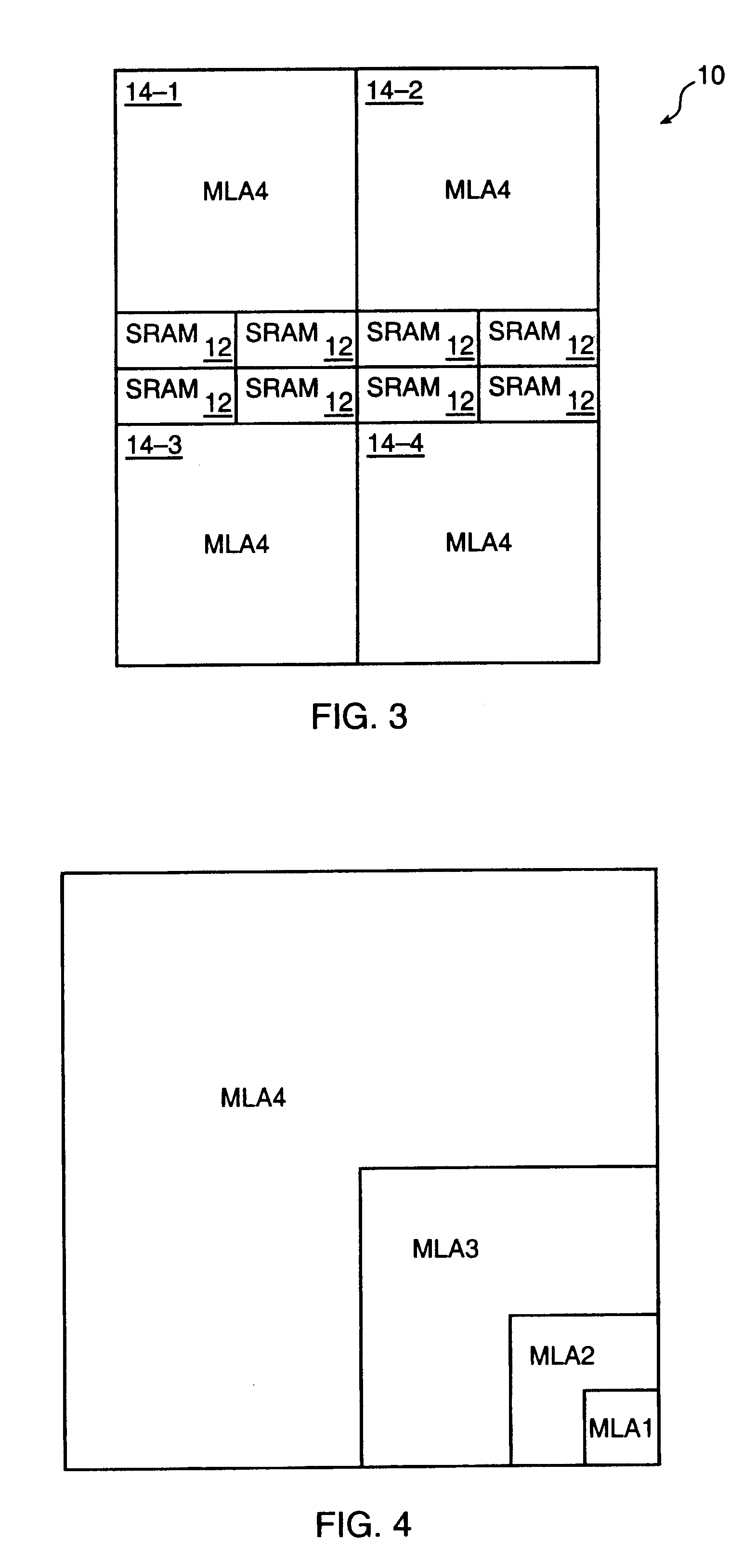
Turning now to FIG. 3, a block diagram of the FPGA core 10 i...


PUM

PropertyMeasurementUnit
densitiesaaaaaaaaaa
flexibleaaaaaaaaaa
flexibilityaaaaaaaaaa

Abstract

An SRAM bus architecture includes pass-through interconnect conductors. Each of the pass-through interconnect conductors is connected to routing channels of the general interconnect architecture of the FPGA through an element which includes a pass transistor connected in parallel with a tri-state buffer. The pass transistors and tri-state buffers are controlled by configuration SRAM bits. Some of the pass-through interconnect conductors are connected by programmable elements to the address, data and control signal lines of the SRAM blocks, while other pass through the SRAM blocks with out being further connected to the SRAM bussing architecture.

Description

1. Field of the InventionThe present invention is related to a field programmable gate array (FPGA) having embedded static random access memory for the embedded SRAM, and the connection of the SRAM bus architecture to the general interconnect architecture of the FPGA.2. The Prior ArtAs integrated circuit technology advances, geometries shrink, performance improves, and densities increase. This trend makes the design of systems of ever increasing complexity at ever decreasing cost feasible. This is especially true in logic products such as Application Specific Integrated Circuits (ASICs), Complex Programmable Logic Devices (CPLDs), and Field Programmable Gate Arrays (FPGAs).The need for integrating fast, flexible, inexpensive memory into these logic products to provide memory for a variety of purposes such as register files, FIFOs, scratch pads, look-up tables, etc. has become more apparent, because there are significant cost and performance savings to be obtained by integrating this...

Claims


Application Information

Patent Timeline
Patent Type & Authority Patents(United States)
IPC IPC(8): C07K14/475C07K14/435C07K14/495H03K19/177
CPCC07K14/475C07K14/495H03K19/17736H03K19/1776
Inventor PLANTS, WILLIAM C.
Owner ACTEL CORP
Why Eureka
Try Eureka