Probe card assembly

a technology of probe card and assembly, which is applied in the field of probe cards, can solve the problems of complex and costly, high cost, and high cost of vertical probe cards, and achieve the effects of avoiding permanent deformation of probes, reducing electrical interference or high-frequency cross talk, and low resistivity

Inactive Publication Date: 2005-02-08
CHIPMOS TECH INC
View PDF9 Cites 42 Cited by
  • Summary
  • Abstract
  • Description
  • Claims
  • Application Information

AI Technical Summary

Problems solved by technology

Conventionally, a vertical probe card comprises a multi-layer printed circuit board, mostly around 30 to 60 wiring layers, which is complex and costly.
The multi-layer printed circuit board is further jointing with an even more costly multi-layer ceramic substrate as a probe head.
The vertical probe card is extremely expensive, and for different IC products, it needs to design the corresponding probe card to meet the special layout of bonding pads of wafer under test.
Moreover, the components of a vertical probe card can not be reused.
Each of the coaxial cable is electrically connected individually, and can not be modularized.
The circuit layers of the substrate can not be reduced, and can only be used for testing low-density electronic products.
This arises the problem that the probe card is not able to precisely position and contact the wafer while in electrical contact at certain temperatures.
However, this conventional coaxial probe card does not have a probe head, and therefore no cantilever needles can be integrated on it.
Furthermore, the coaxial probe card can not have the benefits of modularization to reduce manufacturing cost and lead time.

Method used


Image

  • Probe card assembly
  • Probe card assembly
  • Probe card assembly

Examples


first embodiment

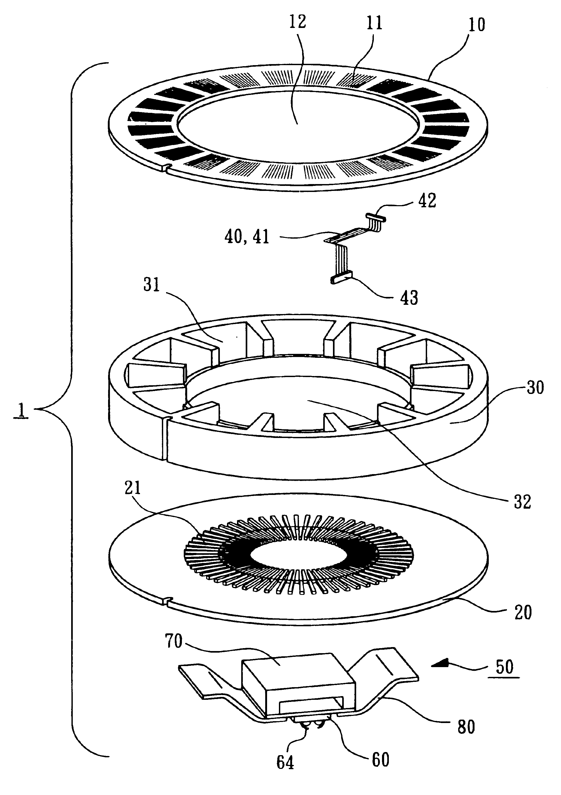
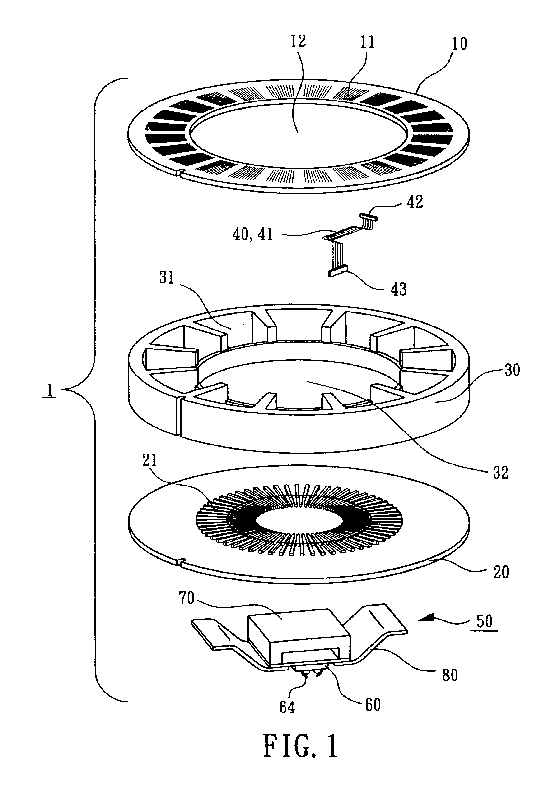
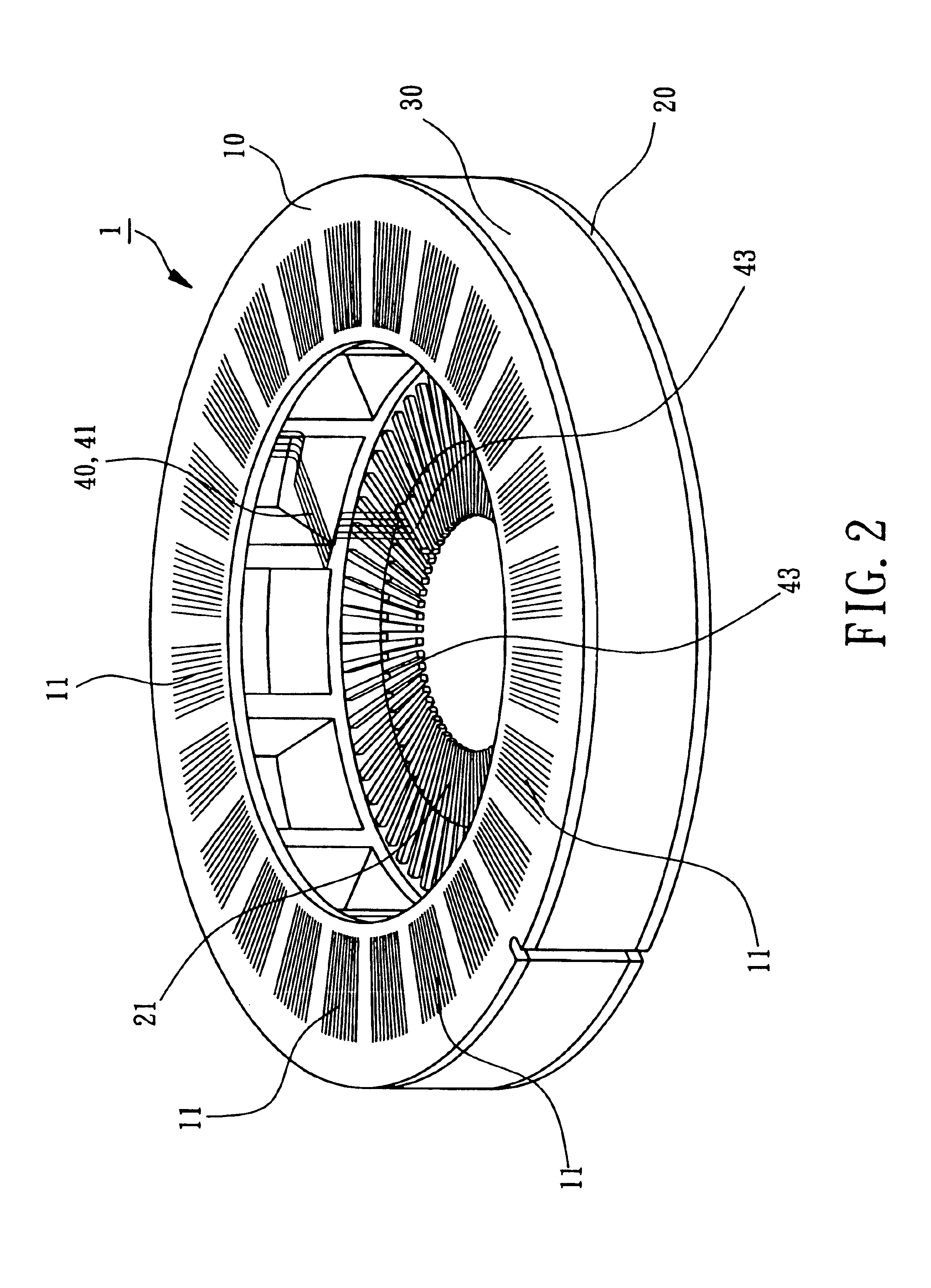
The first embodiment according to the present invention is shown in FIGS. 1, 2, and 3. A probe card assembly 1 is provided to install on the test head of a tester. The probe card assembly is electrically connected to the tester for electrically contacting with the wafer under test, and allows the tester to perform chip probing or wafer sorting on the wafer. The probe card assembly 1 mainly comprises a stiffener ring 30, an upper printed circuit board 10, a lower printed circuit board 20, a modularized probe head 50, and a plurality of coaxial transmitters 40. Wherein the stiffener ring 30 is functioned as a spacer between the upper and lower printed circuit board 10,20, and to enclose the coaxial transmitters 40. The stiffener ring 30 has an upper opening 31 and a lower opening 32 with different size.

The upper printed circuit board 10 is installed on the upper opening 31 of the stiffener ring 30, and functions as a connecting interface between the tester and the probe card. On the o...


PUM


Abstract

A probe card assembly is disclosed. The probe card assembly comprises a stiffener ring combining respectively with an upper printed circuit board and a lower printed circuit board. A plurality of coaxial transmitters are installed in the stiffener ring, and connect to the upper and lower printed circuit boards by cable connectors. The lower printed circuit board is assembled with a detachable probe head which comprises a silicon substrate with probing points and a probe head carrier. A downset is formed at the center of the probe head carrier. The standardized coaxial transmitters, printed circuit boards and probe heads are then assembled as a probe card assembly for testing all sorts of IC products.

Description

FIELD OF THE INVENTIONThe present invention relates to a probe card for wafer testing and, more particularly, to a probe card assembly that is modularized and standardized.BACKGROUND OF THE INVENTIONAfter semiconductor dices are fabricated on a wafer, they will need to go through chip probing or wafer sorting to verify their electrical performance. Usually, the toolings for testing semiconductor wafers are probe cards. A probe card is a tooling which should be manufactured before chip probing or wafer sorting. It is installed on the test head of a tester as an interface between a tester and a wafer under test. Conventionally, a vertical probe card comprises a multi-layer printed circuit board, mostly around 30 to 60 wiring layers, which is complex and costly. The multi-layer printed circuit board is further jointing with an even more costly multi-layer ceramic substrate as a probe head. On the multi-layer ceramic substrate, a plurality of probe needles are formed on an exposed surfa...

Claims


Application Information

Patent Timeline
Patent Type & Authority Patents(United States)
IPC IPC(8): G01R1/073G01R1/02G01R1/18G01R31/28
CPCG01R1/07342G01R1/06733G01R31/2889G01R1/18
Inventor CHENG, SHIH-JYELIU, AN-HONGWANG, YEONG-HERTSENG, YUAN-PINGLEE, YAO-JUNG
Owner CHIPMOS TECH INC
Why Eureka
Try Eureka