Probe apparatus

a technology of probe pins and probes, applied in the direction of individual semiconductor device testing, semiconductor/solid-state device testing/measurement, instruments, etc., can solve the problems of poor contact between the probe pins, inability to properly estimate, and decrease the inspection reliability, so as to improve reliability and increase throughput

Inactive Publication Date: 2005-08-09
TOKYO ELECTRON LTD
View PDF5 Cites 75 Cited by
  • Summary
  • Abstract
  • Description
  • Claims
  • Application Information

AI Technical Summary

Benefits of technology

[0008]It is, therefore, an object of the present invention to provide a probe apparatus capable of performing the inspection with improved reliability and increased throughput by way of detecting the Z directional displacement of the probe card during the inspection stage and stabilizing the contact load between the probe pins and the objects to be inspected.

Problems solved by technology

As a result, the Z directional distance (Z vertical distance) between the probe pins 8a and the electrode pads of the wafer W can be varied by, e.g., 100 μm, causing poor contacts between the probe pins 8a and the electrode pads of the wafer W and decreasing inspection reliability.
However, even in such a case where the probe card 8 is preheated and the wafer W is put into the pseudo-contact state prior to the actual inspection stage, the Z directional displacement of the probe card 8 due to a thermal deformation caused by additional heating during the actual inspection stage and that due to a contact load urged thereto during the inspection stage cannot be properly estimated.
Accordingly, an excess or deficiency may occur in the contact load between the probe pins 8a and the electrode pads of the wafer W, to thereby lower the inspection reliability.
Furthermore, a considerable amount of time (e.g., 1˜2 hours) may be required for the probe card 8 to become thermally stable, leading to a significant decrease in throughput.

Method used


Image

  • Probe apparatus
  • Probe apparatus
  • Probe apparatus

Examples


Embodiment Construction

[0017]Preferred embodiments of the present invention will now be described in detail with reference to FIGS. 1 to 4, in which like parts are denoted by like reference numerals.

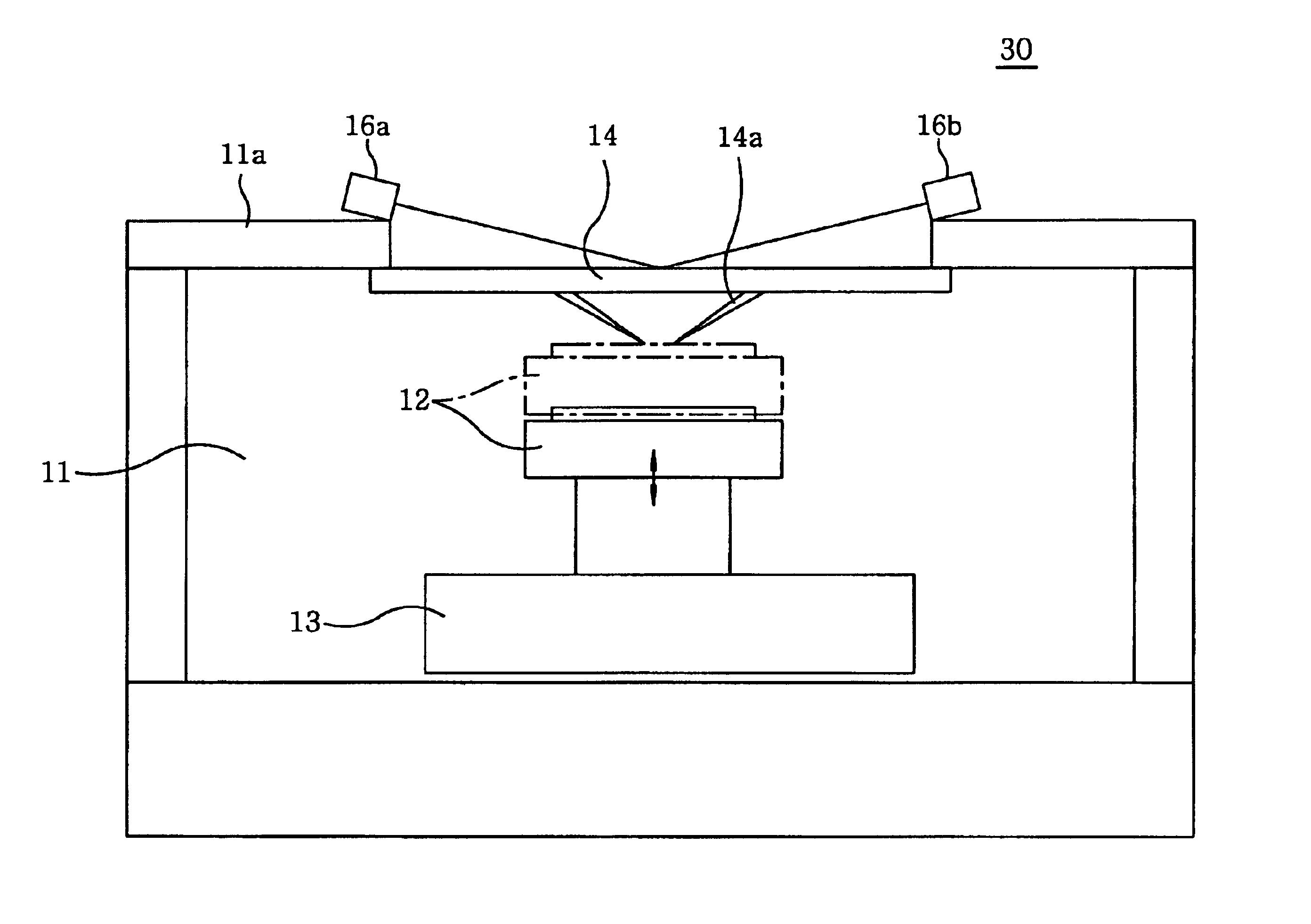
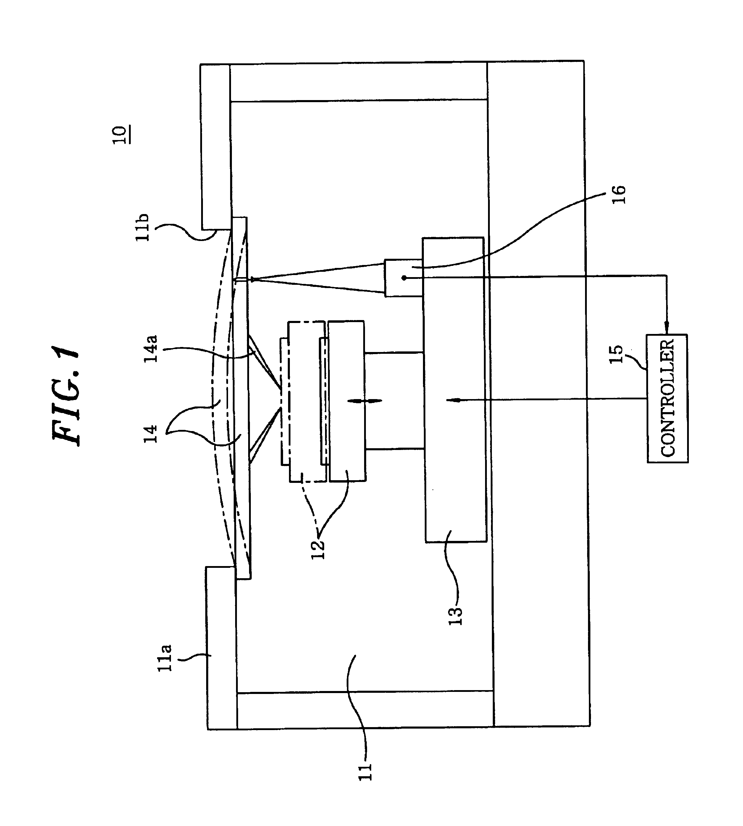
[0018]As shown in FIG. 1, a probe apparatus 10 of a first preferred embodiment includes, as in the conventional one shown in FIGS. 5A and 5B, a main chuck 12 which is situated inside a prober chamber 11 and is vertically moved in a Z direction by an elevating mechanism (not shown) embedded therein; an XY table 13 which moves the main chuck 12 in X and Y directions; a probe card 14 which is arranged above the main chuck 12; an alignment mechanism (not shown) which aligns the probe card 14 with a wafer W mounted on the main chuck 12; and a controller 15 which controls driving mechanisms thereof. The probe card 14 is fixed at an opening 11b of a head plate 11a of the prober chamber 11.

[0019]When the wafer W is inspected, the alignment mechanism and the XY table 13 cooperate to align the wafer W mounted on the mai...


PUM


Abstract

A probe apparatus includes a mounting member on which an object to be inspected is mounted and a temperature thereof is being adjusted, a probe card arranged opposite to the mounting member, a driving mechanism which changes a relative positional relationship between the mounting member and the probe card, and a sensor which detects the distance between the sensor and the probe card. By way of detecting the height of the deformed probe card through the use of the sensor and revising the elevation distance of the mounting member, the electrode pads of the wafer W and the probe pins can electrically contact each other with a stable pin pressure, providing high inspection reliability and an increase in throughput.

Description

FIELD OF THE INVENTION[0001]The present invention relates to a probe apparatus; and, more particularly, to a probe apparatus capable of providing an enhanced inspection reliability.BACKGROUND OF THE INVENTION[0002]FIGS. 5A and 5B illustrate a conventional probe apparatus used for inspecting electrical characteristics of, e.g., devices formed on a wafer during the manufacture of the devices. As shown in FIGS. 5A and 5B, the probe apparatus includes a loader chamber 1 for loading a wafer W and a prober chamber 2 for inspecting electrical characteristics of the wafer W conveyed from the loader chamber 1. The loader chamber 1 includes a cassette table 3, a wafer convey mechanism 4 for conveying the wafer W to the prober chamber 2, and a sub-chuck 5 for pre-aligning the wafer W with reference to an orientation flat or a notch thereof during the process of conveying the wafer W via the wafer convey mechanism 4.[0003]Further, the prober chamber 2 includes a temperature controllable main ch...

Claims


Application Information

Patent Timeline
Patent Type & Authority Patents(United States)
IPC IPC(8): G01R31/28G01B21/02G01R31/26H01L21/66
CPCG01R31/2891G01R31/2887G01R31/2806H01L22/00
Inventor YOSHIOKA, HARUHIKO
Owner TOKYO ELECTRON LTD
Why Eureka
Try Eureka