Silicon wafer probe station using back-side imaging

Inactive Publication Date: 2003-02-04
INFRARED LAB
View PDF3 Cites 79 Cited by
  • Summary
  • Abstract
  • Description
  • Claims
  • Application Information

AI Technical Summary

Problems solved by technology

Thus, the full power of IR microscopy has been limited to packaged parts.
Several disadvantages characterize this prior-art approach.
In addition, current top-side imaging is limited to contact pads that are positioned at the edges of the integrated circuit in order to provide room for the viewing port through the probe card.
Thus, recently introduced "flip-chip" probe cards, which have probe tips designed to match contact pads located throughout the interior of the chip, cannot be aligned with conventional top-side imaging.
The relative lack of access to a clear view of all probe tips afforded by the prior art also prevents a determination of their precise spatial position and an adjustment of their planar attitude with

Method used


Image

  • Silicon wafer probe station using back-side imaging
  • Silicon wafer probe station using back-side imaging
  • Silicon wafer probe station using back-side imaging

Examples


Embodiment Construction

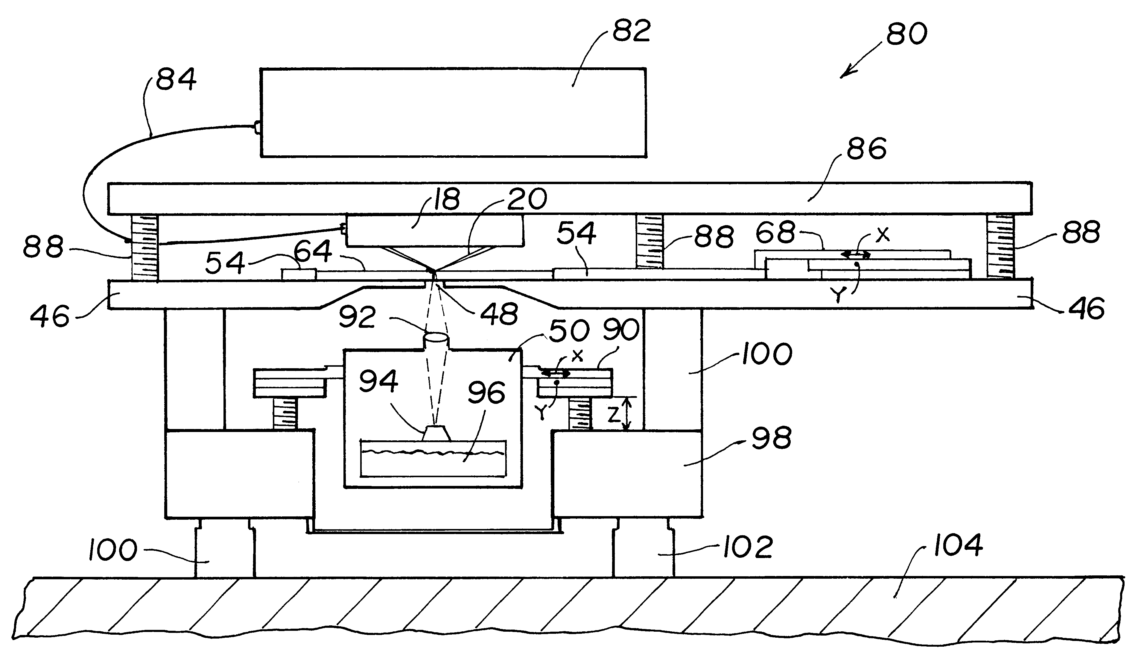
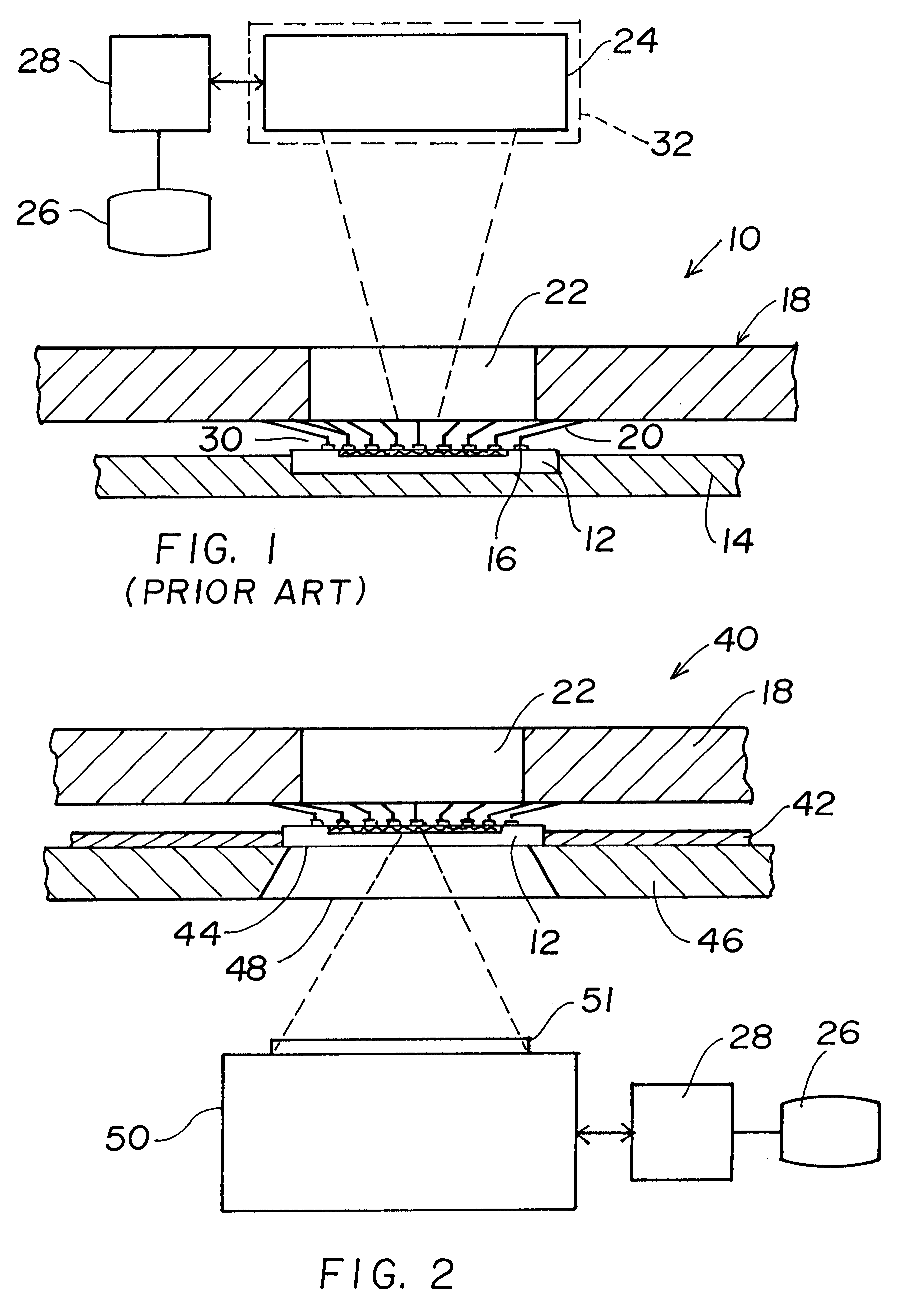
The silicon material constituting the substrate of substantially all integrated circuits is transparent to wavelengths in the infrared range. Accordingly, this invention is based on the idea of utilizing an infrared camera to "see" through the silicon substrate of the integrated circuit from the bottom of the chip in order to align the contact pads with the tips of a probe card. Moreover, the same infrared camera can be used to image infrared hot-carrier and thermal emissions resulting from circuit faults for the purpose of failure analysis.

It is noted that the embodiments of the present invention are described with reference to x, y and z orthogonal coordinates wherein x and y define a horizontal plane parallel to the plane of the integrated circuit and z defines a vertical direction orthogonal to such plane, but it is obvious that the structure and operation of the features detailed herein could be rotated in any direction with equivalent results. The terms top and front are used ...


PUM


Abstract

A back-side imaging infrared microscope is integrated with a novel integrated-circuit probe station. The microscope is located below the silicon substrate of the integrated circuit, on the side opposite to the probe card. The electronic circuitry located on the top side of the substrate is imaged through the back side of the substrate and through a window sized to provide a view of a single integrated circuit and of the corresponding probe tips overlying the contact pads. Since the silicon substrate of integrated circuits is transparent to infrared wavelengths, the alignment between probe tips and contact pads is carried out with a clear view of both from the bottom of the substrate. Furthermore, emission images from the integrated circuit are taken during testing with the same microscope after electrical contact has been established.

Description

1. Field of the InventionThis invention is related in general to the field of electronic microscopes and cameras for testing integrated circuits in wafer or chip form. In particular, the invention concerns the use of an infrared microscope for imaging and aligning the probe tips of a conventional probe card with the electrical contact pads of the integrated circuit. It also enables more advanced probe cards to be used with flip-chip technology.2. Description of the Related ArtConventional testing of integrated circuits (ICs) is carried out on an individual IC at the wafer level by contacting the electrical contact pads of the IC with the finger tips of a probe card facing the top side of the circuit. The probe card energizes the circuit and performs diagnostic tests that enable the detection of faults, which may then be specifically identified with further testing performed on individually mounted chips. For example, recent advances in the art have been obtained by using an infrared...

Claims


Application Information

Patent Timeline
IPC IPC(8): G01N21/95G01N21/88G01R31/311G01R31/28
CPCG01N21/9501G01R31/311G01R31/2831
Inventor LOW, FRANK J.
Owner INFRARED LAB
Why Eureka
Try Eureka