Apparatus And Method For Limiting Over Travel In A Probe Card Assembly

a probe card and assembly technology, applied in the field of testing semiconductor devices, can solve the problems of bad dies, non-full functionalities, and good dies

Inactive Publication Date: 2006-11-23
FORMFACTOR INC
View PDF32 Cites 75 Cited by
  • Summary
  • Abstract
  • Description
  • Claims
  • Application Information

AI Technical Summary

Problems solved by technology

In practice, physical defects in the wafer itself and / or defects in the processing of the wafer often lead to some of the dies being “good” (fully functional) and some of the dies being “bad” (non-fully functional).

Method used


Image

  • Apparatus And Method For Limiting Over Travel In A Probe Card Assembly
  • Apparatus And Method For Limiting Over Travel In A Probe Card Assembly
  • Apparatus And Method For Limiting Over Travel In A Probe Card Assembly

Examples


Embodiment Construction

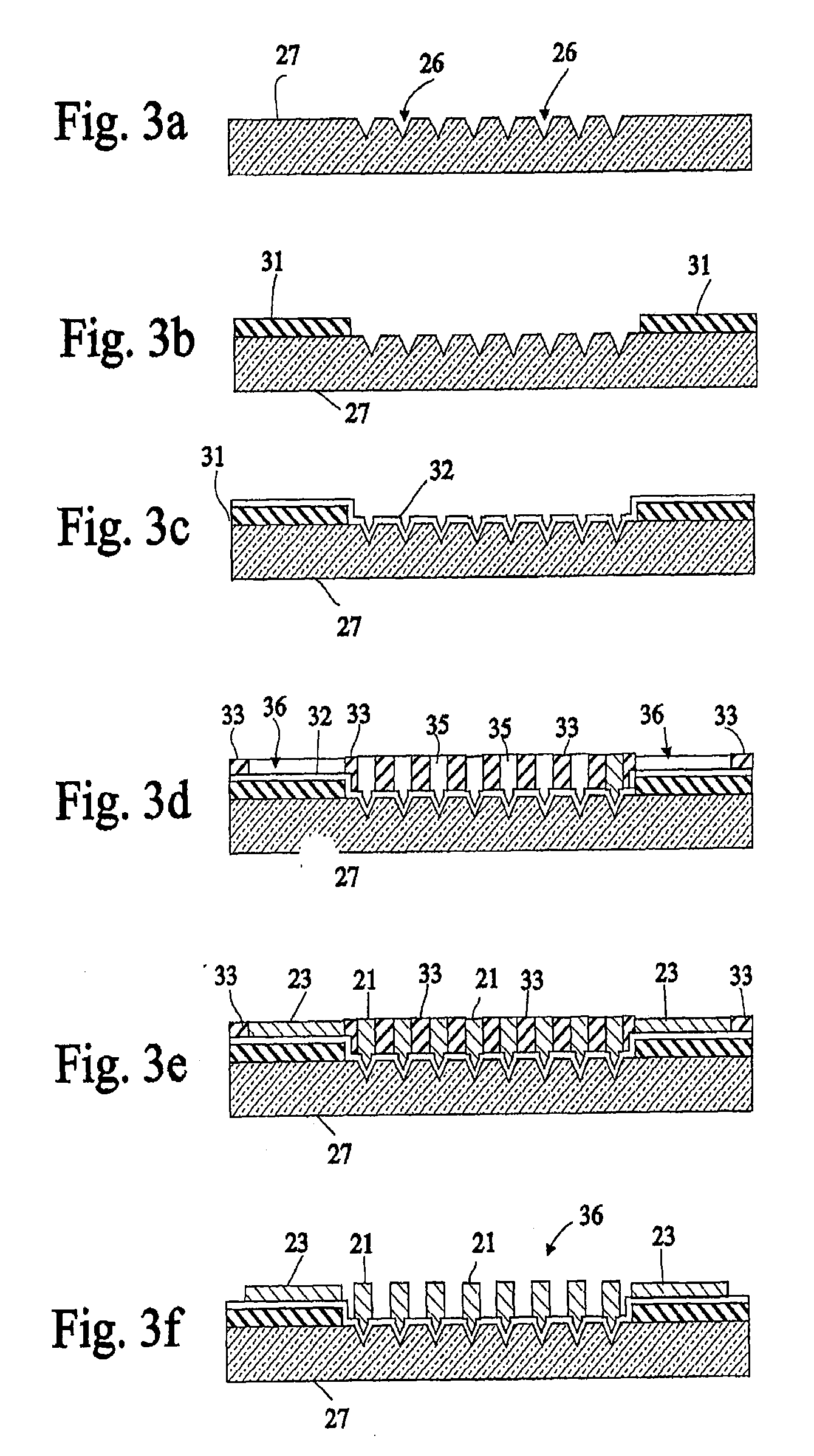
[0018] For the purposes of promoting an understanding of the principles of the invention, reference will now be made to the embodiments illustrated in the drawings and specific language will be used to describe the same. It will nevertheless be understood that no limitation of the scope of the invention is thereby intended, and any alterations or modifications in the illustrated device, and any further applications of the principles of the invention as illustrated therein are contemplated as would normally occur to one skilled in the art to which the invention relates.

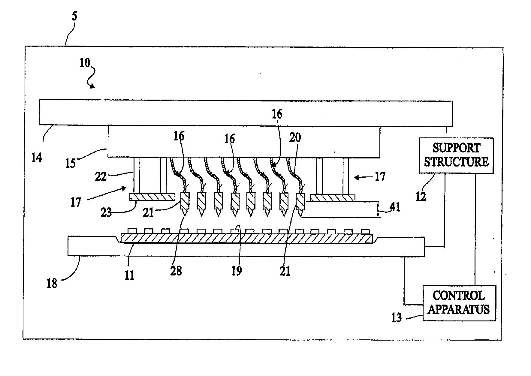
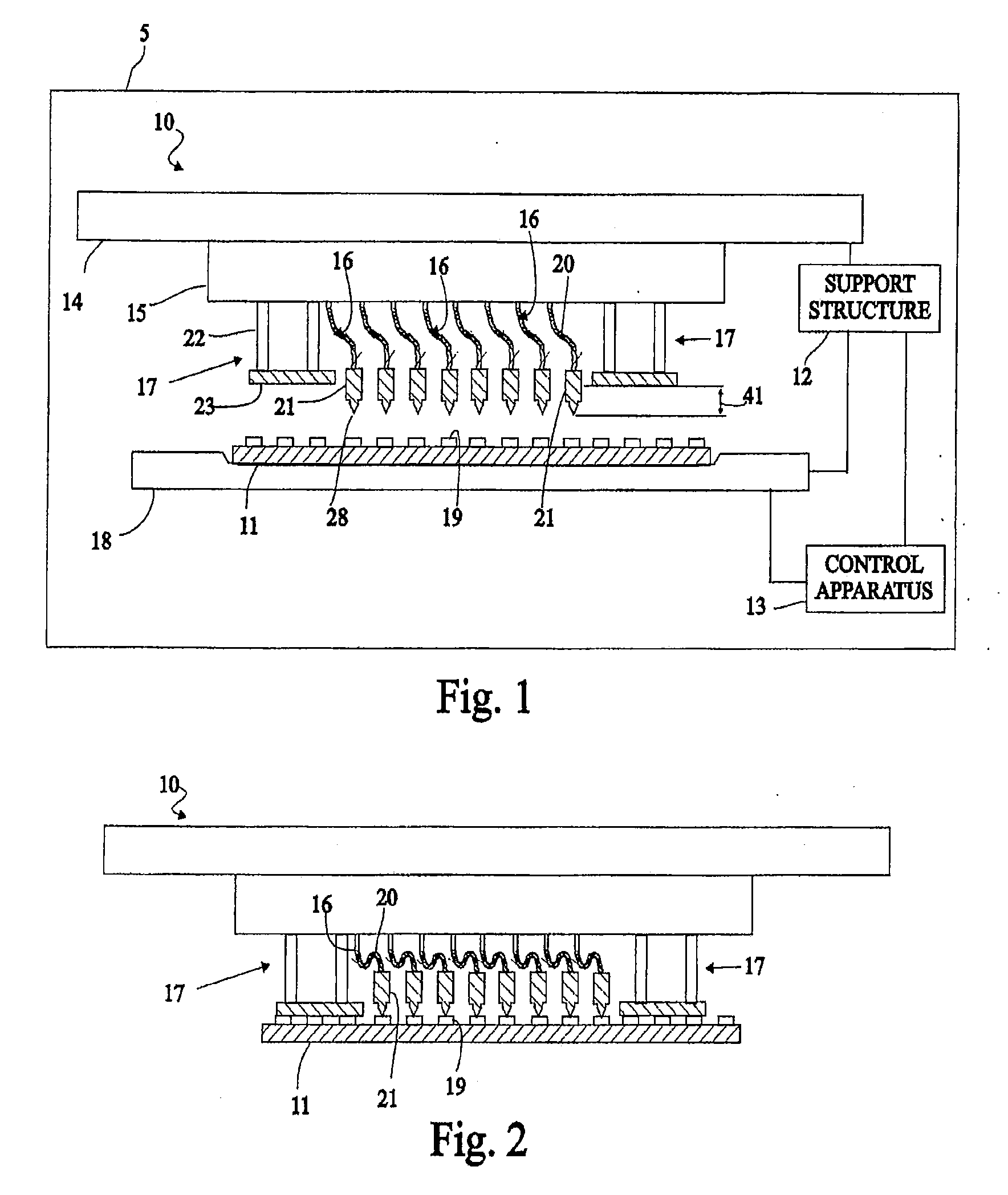
[0019] Referring to FIG. 1, there is shown a semiconductor tester 5 for testing semiconductor devices. Tester 5 generally includes a probe card assembly 10, support structure 12, control apparatus 13 and a semiconductor device holder 18. Probe card assembly 10 is shown positioned to engage with and test a semiconductor device 11 (otherwise known as a device under test or “DUT”) in accordance with the present invention...


PUM


Abstract

Methods and apparatuses for testing semiconductor devices are disclosed. Over travel stops limit over travel of a device to be tested with respect to probes of a probe card assembly. Feedback control techniques are employed to control relative movement of the device and the probe card assembly. A probe card assembly includes flexible base for absorbing excessive over travel of the device to be tested with respect to the probe card assembly.

Description

FIELD OF THE INVENTION [0001] The present invention relates to testing semiconductor devices. BACKGROUND OF THE INVENTION [0002] Individual semiconductor (integrated circuit) devices (dies) are typically produced by creating several identical devices on a semiconductor wafer using known techniques of photolithography, deposition, diffusion and the like. These processes are intended to create a plurality of fully functional integrated circuit devices, after which the individual dies are singulated (severed) from the semiconductor wafer. In practice, physical defects in the wafer itself and / or defects in the processing of the wafer often lead to some of the dies being “good” (fully functional) and some of the dies being “bad” (non-fully functional). It is generally desirable to be able to identify which of the plurality of dies on the wafer are good dies prior to their packaging (encapsulation within a transfer-molded plastic, ceramic or metal package for subsequent integration into a...

Claims


Application Information

Patent Timeline
Patent Type & Authority Applications(United States)
IPC IPC(8): G01R31/02G01R3/00G01R31/28
CPCG01R3/00G01R31/2887G01R31/2886G01R1/07357G01R1/06G01R31/26H01L22/00
Inventor COOPER, TIMOTHY E.ELDRIDGE, BENJAMIN N.REYNOLDS, CARL V.SHENOY, RAVINDRA VAMAN
Owner FORMFACTOR INC
Why Eureka
Try Eureka