Needle assembly of probe card

a technology of probe card and needle, which is applied in the direction of measurement devices, semiconductor/solid-state device testing/measurement, instruments, etc., can solve the problems of complicated and delicate process techniques, shorten the transmission path of electric signals,

Inactive Publication Date: 2005-07-26
YULIM HITECH
View PDF7 Cites 80 Cited by
  • Summary
  • Abstract
  • Description
  • Claims
  • Application Information

AI Technical Summary

Benefits of technology

[0012]One feature of the present invention provides a needle assembly of a probe card that is appropriately employed for testing high integrated and miniaturized semiconductor devices according to a current technical tendency, by making the thickness of needles and spacing between the needles smaller.
[0013]Another feature of the present invention is to provide a probe card to reduce the number of assembling processes and increase productivity by unifying needles being contacted with electrode pads of a semiconductor device and components supporting the needles into a needle assembly.

Problems solved by technology

As a result, such conventional test apparatuses of the semiconductor devices decrease interval or spacing between needles, and also shorten the transmission path of electric signals, when the needles contact an electrode pad of the semiconductor device from a main substrate.
A very complicated and delicate process technique is therefore needed to realize this configuration.

Method used


Image

  • Needle assembly of probe card
  • Needle assembly of probe card
  • Needle assembly of probe card

Examples


Embodiment Construction

[0021]The present invention and exemplary embodiments thereof are more fully described below with reference to the accompanying drawings. This invention may, however, be embodied in many different forms and should not be construed as being limited to the exemplary embodiments set forth herein; rather, these exemplary embodiments are provided so that this disclosure is thorough and complete, and conveys the concept of the invention to those skilled in the art.

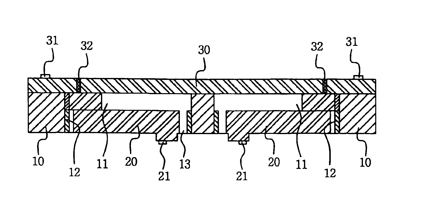
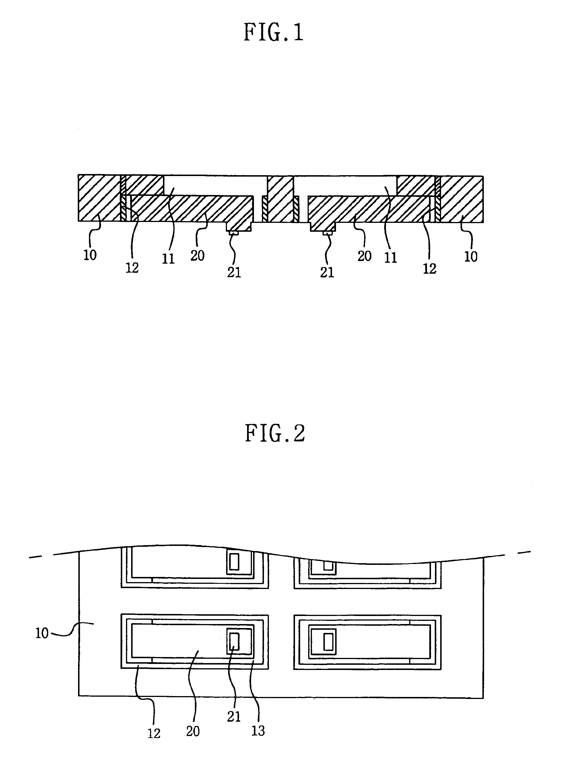
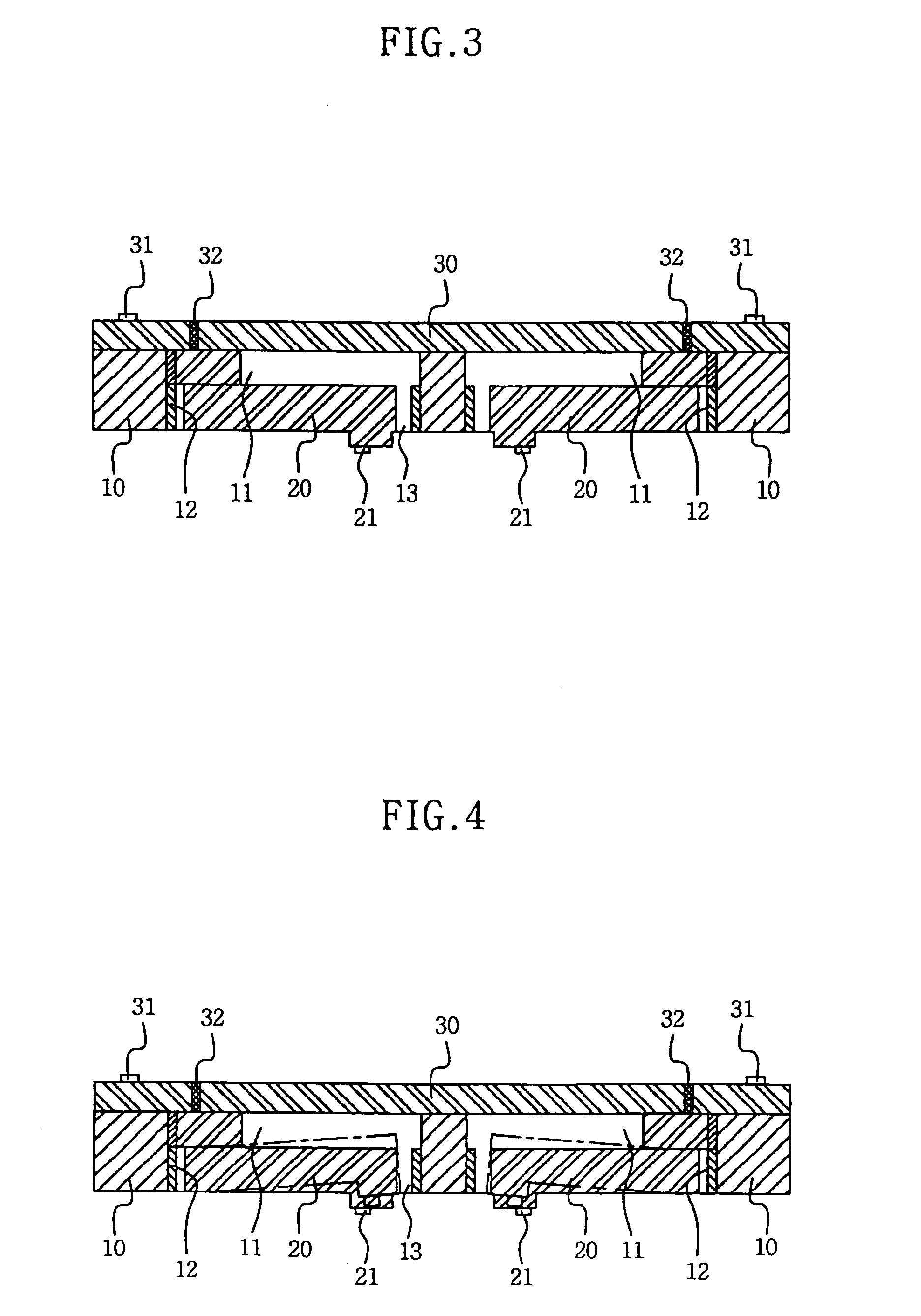
[0022]FIG. 1 is a cross-sectional view illustrating a needle assembly of a probe card for use in a characteristic test of a semiconductor device according to one exemplary embodiment of the present invention.

[0023]A needle assembly of the invention has inventive characteristics that a plate 10 and a needle 20 are integrated into one body.

[0024]It is desirable that the plate 10 be made of silicon material and the needle 20 be made of conductive material that is proper to a unified formation with the plate 10.

[0025]Describing more...


PUM


Abstract

A needle assembly of probe card includes a plate and needles formed therein for enhancing an assembly characteristic and productivity and increasing an exact and reliable characteristic test. The plate is provided with holes that are formed with an insulating film on an inner side surface thereof. One side end surface of the needle adheres on an inner side surface of the hole, another side end surface thereof is spaced from an inner side surface of the hole, and a vertical thickness of the other side of the hole is formed thinner than the plate so as to have a space in which the other side can vertically move upwardly and downwardly. The plate and the needle are integrated.

Description

PRIORITY[0001]This application claims priority to an application entitled “Needle Assembly of Probe Card” filed in the Korean Industrial Property Office on Apr. 11, 2003 and assigned Serial No. 2003-22937, the contents of which are incorporated herein by reference.FIELD OF THE INVENTION[0002]The present invention relates to a characteristic test for semiconductor devices, and more particularly, to a needle assembly of probe card for performing a stabilized characteristic test for miniaturized and high-integrated semiconductor devices.DESCRIPTION OF THE RELATED ART[0003]Semiconductor devices are generally manufactured through fabrication processes for forming patterns on wafers and assembly processes for assembling the pattern-formed wafers into respective chips.[0004]Between the fabrication processes and the assembly processes, an electrical die sorting (hereinafter, referred to as ‘EDS’) process is generally performed to test electrical characteristics of the respective chips forme...

Claims


Application Information

Patent Timeline
Patent Type & Authority Patents(United States)
IPC IPC(8): G01R1/073H01L21/66G01R31/26
CPCG01R1/07357
Inventor JUN, TAE-UN
Owner YULIM HITECH
Why Eureka
Try Eureka