Contactor and production method for contractor

a production method and contactor technology, applied in the field of contactors and production methods for contractors, can solve the problems of low freedom with which the probe needles were arranged, affecting the stability of the probe terminal, and affecting the accuracy of the probe, so as to achieve a higher degree of freedom and lessen the influence of thermal ad

Inactive Publication Date: 2002-02-05
TOKYO ELECTRON LTD
View PDF12 Cites 80 Cited by
  • Summary
  • Abstract
  • Description
  • Claims
  • Application Information

AI Technical Summary

Benefits of technology

The present invention solves the above-mentioned tasks. The present invention can ensure a higher degree of freedom with which the probe terminals are arranged. According to the present invention, the probe terminals can be easily so arranged as to correspond to any electrode array of the ...

Problems solved by technology

In a conventional probe card, a plurality of probe terminals are supported at one-end sides and, in the case where electrode pads on an object (IC chip) to be checked are arranged in a plurality of arrays, a support structure of those probe terminals corresponding to this arrangement becomes very complicated.
It has been difficult...

Method used


Image

  • Contactor and production method for contractor
  • Contactor and production method for contractor
  • Contactor and production method for contractor

Examples


Embodiment Construction

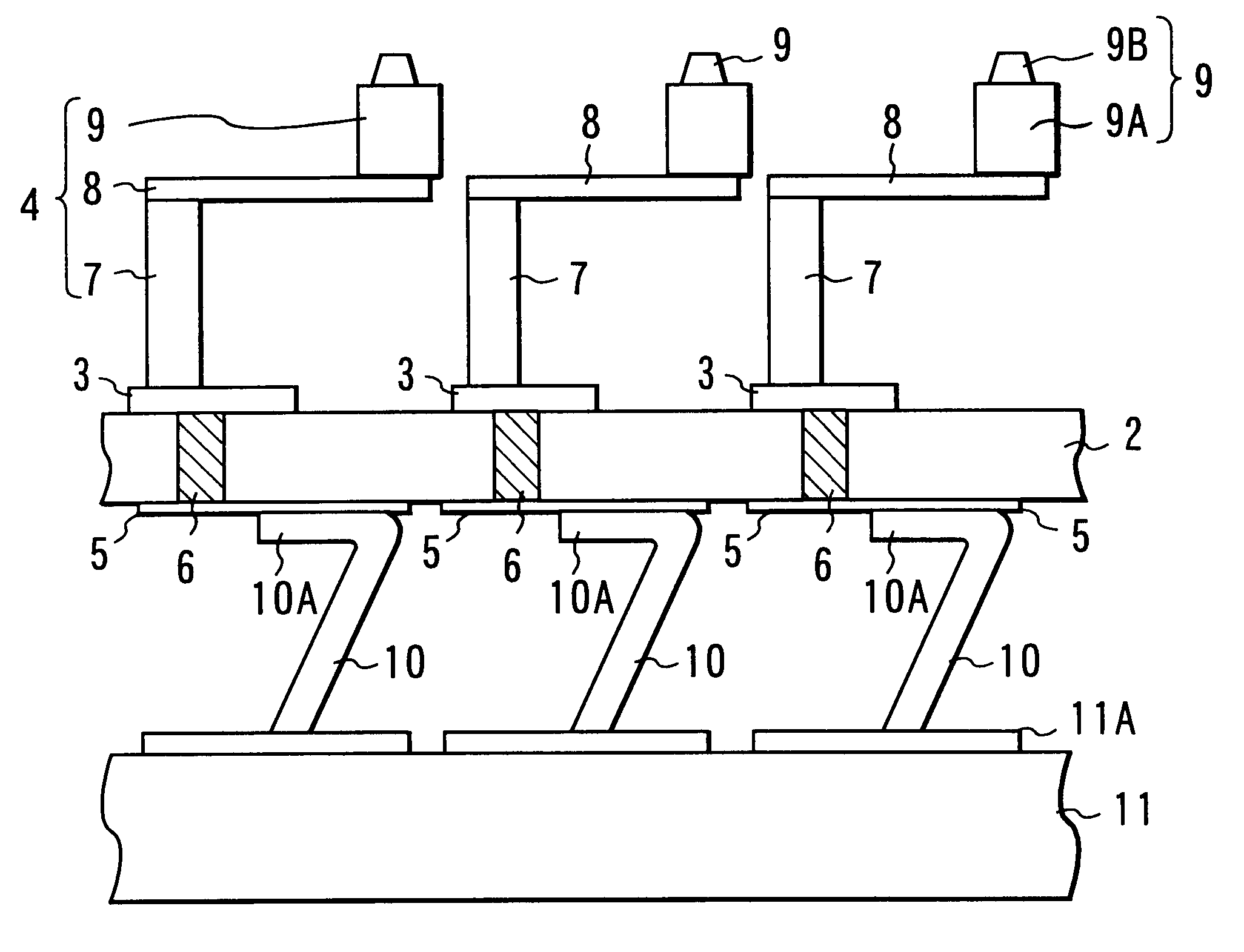
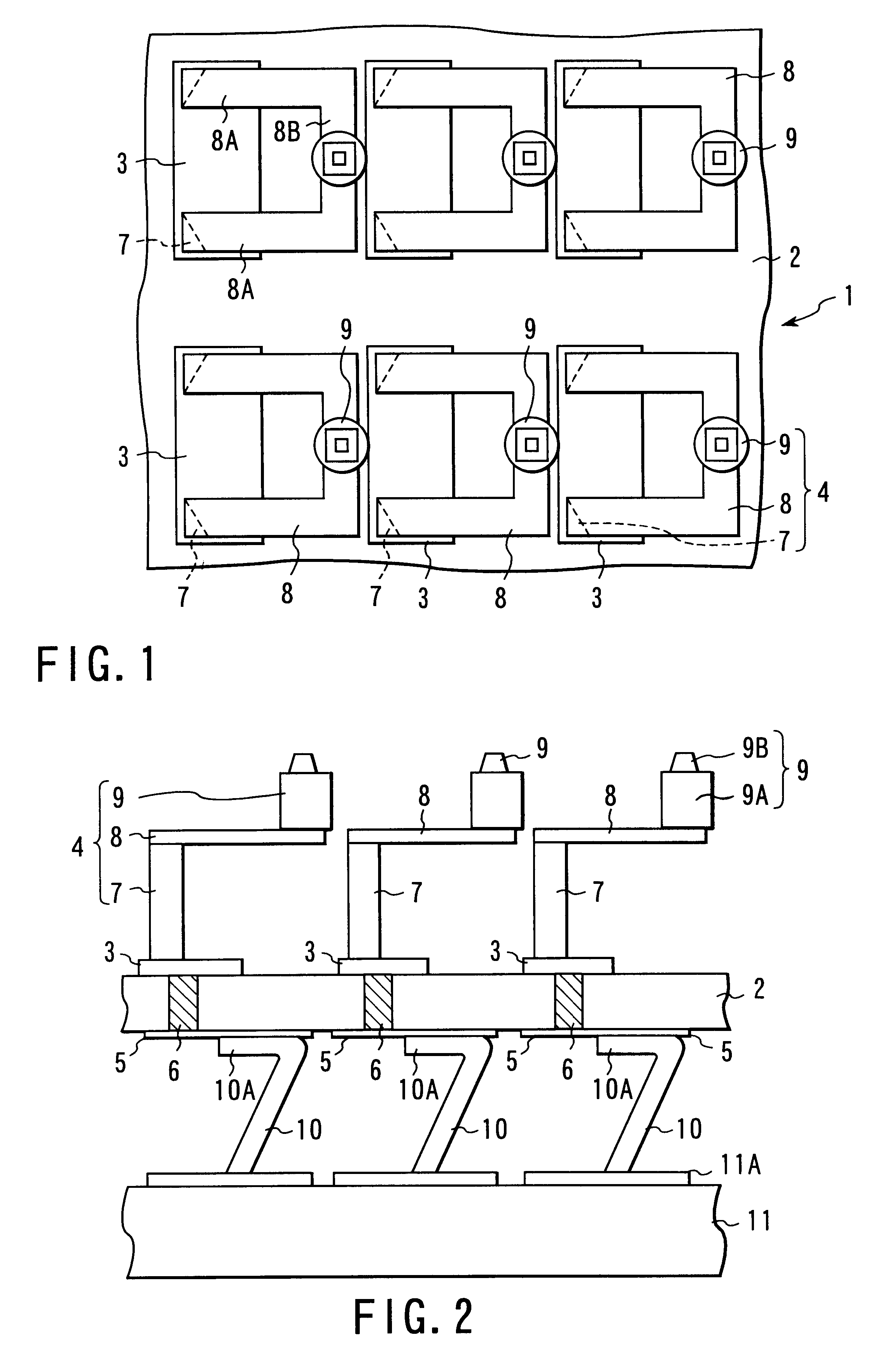
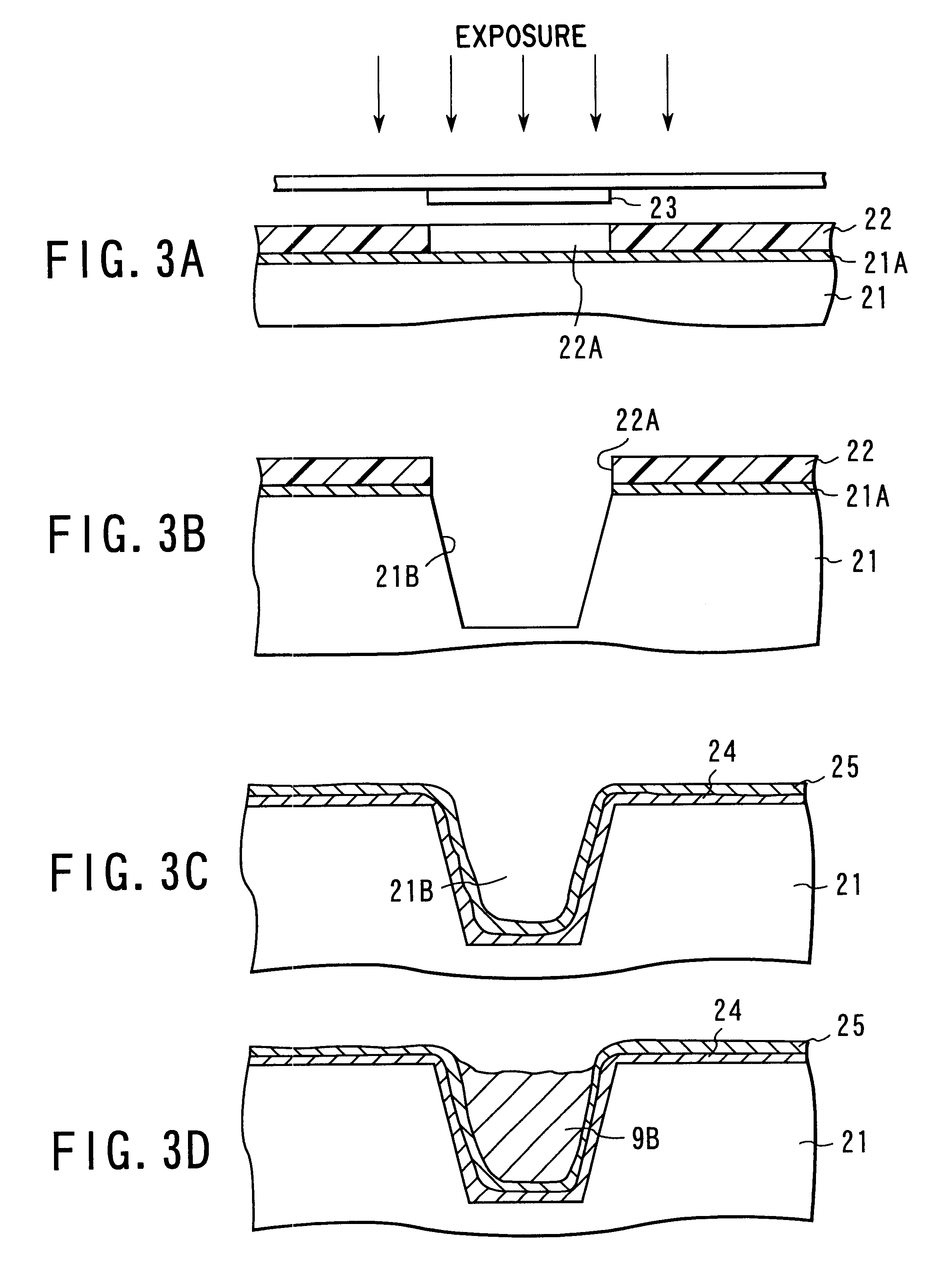
The present invention will be explained below on the basis of a first embodiment shown in FIGS. 1 to 6. The present invention relates to a contactor usable in checking the electrical characteristics of a to-be-checked object having electrode pads for checking. As this object, there are a plurality of IC chips formed on a semiconductor wafer, various kinds of electrical components and electrical products such as a liquid crystal. Here, an explanation will be made about a case where a plurality of IC chips formed on the semiconductor wafer are taken as the object to be checked.

The contactor of the present embodiment is shown in FIGS. 1 and 2. As a first substrate 2 having a size substantially equal to the object (wafer) to be checked a silicon substrate 2 can be adopted. First electrodes 3 are arranged over a whole surface of the first substrate 2 to correspond to a plurality of checking electrode pads of the object. As an array of the first electrodes, for example, a matrix array can...


PUM


Abstract

A conventional probe card is very complex in a support structure of probe terminals and it has been difficult to change an array of the probe terminals correspondingly to various arrays of electrode pads of an object to be checked. A contactor (1) of the present invention simultaneously sets its probe terminals in contact with a plurality of electrode pads of an object to be checked and electrical checking of the object is made once or a plurality of times. It has a plurality of first electrodes (3) arranged on a first substrate (silicon substrate) (2) and probe terminals (4) respectively provided on these electrodes (3). The probe terminal (4) has a conductive support (7) provided on the first electrode, elastic support plate (8) whose one end is fixed to the upper end of the conductive support column (7), and probe terminal (bump) 9 fixed to the free end portion of the elastic support plate (8).

Description

The Present invention relates to a contactor used in checking the electrical characteristic of an object to be checked. In particular, the present invention relates to a contactor used in checking the electrical characteristics of a plurality of semiconductor elements formed on a semiconductor wafer.As a contactor used in checking the electrical characteristics of a larger number of IC chips of a memory circuit, logic circuit, etc., formed on, for example, a semiconductor wafer (hereinafter referred to simply as a wafer), use is made of a probe card. The probe card has a plurality of probe terminals (for example, probe needles, bumps) corresponding to a plurality of electrode pads formed on, for example, an IC chip. The probe card has its probe terminals set in contact with electrode pads of an object to be checked and, by doing so, it serves as a relay for transmitting and receiving checking signals between a testing apparatus and the object to be checked.In a recent time, the inte...

Claims


Application Information

Patent Timeline
IPC IPC(8): G01R1/073G01R1/067G01R3/00
CPCG01R1/06727G01R3/00G01R1/07342G01R1/06711G01R1/06716
Inventor HAGIHARA, JUNICHIIINO, SHINJI
Owner TOKYO ELECTRON LTD
Why Eureka
Try Eureka