Mount for semiconductor light emitting device

a technology of light-emitting devices and mounting brackets, which is applied in the direction of solid-state devices, printed circuit assembling, printed circuit manufacturing, etc., can solve the problems of how much heating the wire-bonds can endure, the p-contact generally transmits light poorly, and the heat resistance of the wire-bonds is high

Inactive Publication Date: 2005-04-05
LUMILEDS
View PDF9 Cites 157 Cited by
  • Summary
  • Abstract
  • Description
  • Claims
  • Application Information

AI Technical Summary

Problems solved by technology

Since the p-contact typically includes a metal and / or a semi-transparent metal oxide in order to optimize its electrical conduction properties, the p-contact generally transmits light poorly, posing a design problem.
First, the wire bonds are sensitive to heat.
One of the limitations of the LED design is thus how much heating the wire-bonds can endure.
This issue becomes more and more important as newer generations of LEDs are planned to be operated at higher power and in higher temperature environments, leading to an increase in operating temperatures and heat production.
Elevated temperatures and repeated thermal cycling can lead to damage to the wire bond, such as separation of the ball from the solderable layer, brittleness in the wire, or breakage in the wire caused by melting at a narrow cross section.
Such heating problems can also occur in case of an electrostatic discharge (“ESD”), or during transient periods, such as switching the device on and off.
Elevated temperature operation can also lead to enhanced growth of physically brittle and electrically resistive intermetallic phases at the interface between balls 126 and solderable layers 118, which can ultimately cause failure at the interface.
However, a sizeable fraction of the recombination may be non-radiative, generating heat instead.
Third, the wires are fragile and thus are usually the primary failure mechanism under extreme operating conditions, such as temperature shocks, rough handling, and high humidity environments.
Fourth, wire-bonds require space on the submount outside the footprint of the LED, resulting in bigger and more expensive devices.
Light emitted by the LED and incident on the large submount may be reflected from the submount, undesirably increasing the size of the light source.
Finally, wire-bonds can trap air in the package during subsequent encapsulation of the LED, creating large steps in index of refraction which may reduce the efficiency with which light is extracted from the LED die into the outside world.

Method used


Image

  • Mount for semiconductor light emitting device
  • Mount for semiconductor light emitting device
  • Mount for semiconductor light emitting device

Examples


Embodiment Construction

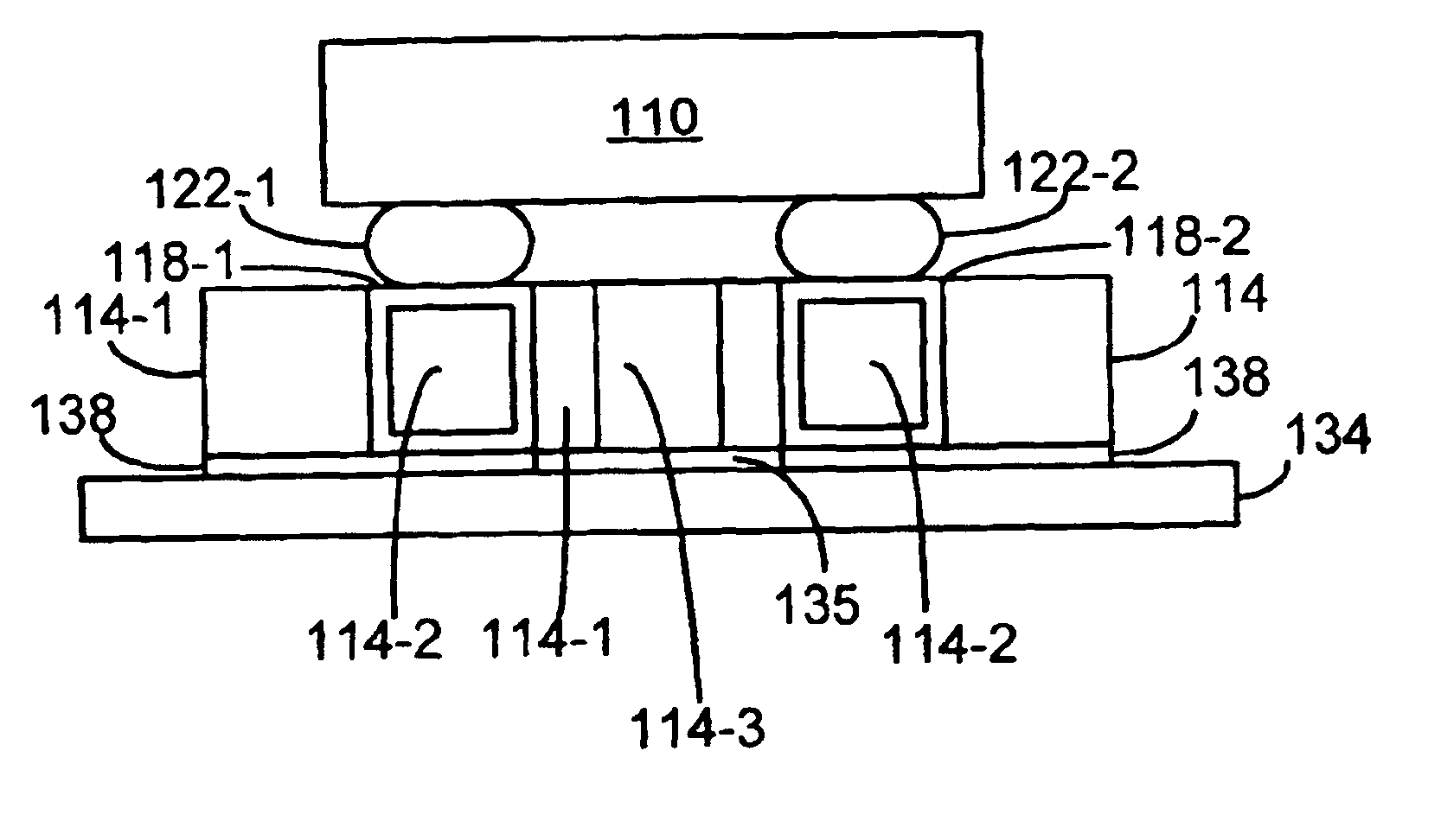
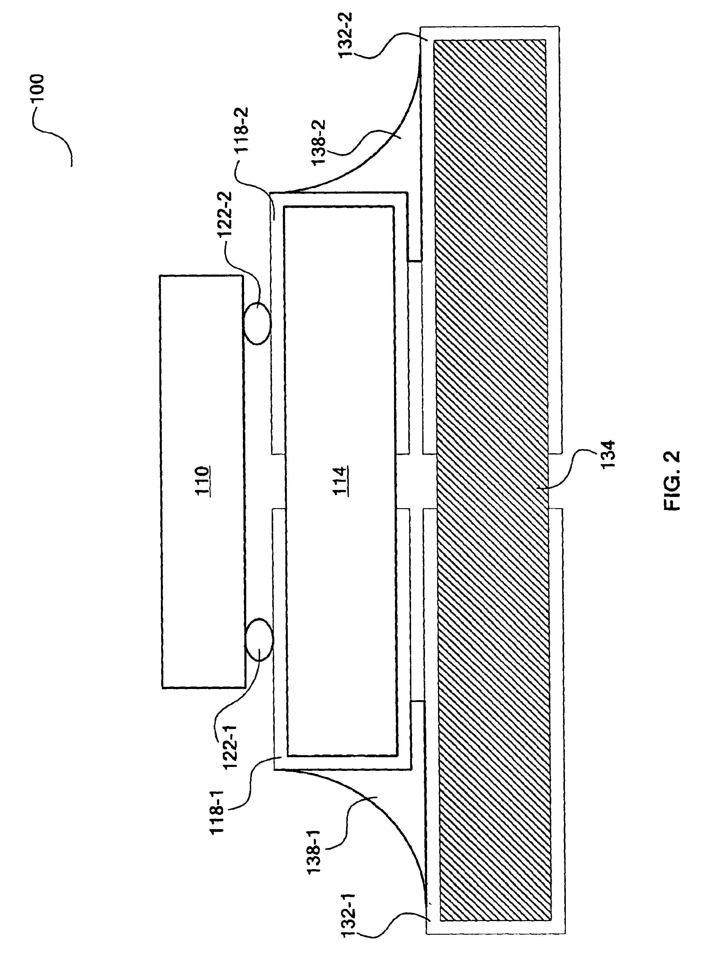
According to embodiments of the invention, the submount on which an LED is mounted has electrical contacts on the side opposite the LED, such that the LED and submount are surface-mountable on another device, such as a board, by solder joints instead of wire bonds.

FIG. 2, illustrates an embodiment of the invention with solder joints. Electrical contacts for the die 110 of the light emitting device 100 are formed by coupling interconnects 122-1 and 122-2 to the die. Although the illustrated embodiments refer to solder balls, the interconnects may be made of elemental metals, metal alloys, semiconductor-metal alloys, solders, thermally and electrically conductive pastes or compounds (e.g., epoxies), eutectic joints (e.g., Pd-In-Pd) between dissimilar metals between the LED die and submount, Au stud-bumps, or configurations of solder besides balls, such as bars. In different embodiments the number of solder balls can be three or higher. Three solder ball designs provide a stable suppor...


PUM


Abstract

A device includes a submount, and a semiconductor light emitting device mounted on first and second conductive regions on a first side of the submount in a flip chip architecture configuration. The submount has third and fourth conductive regions on a second side of the submount. The third and fourth conductive regions may be used to solder the submount to structure such as a board, without the use of wire bonds. The first and third conductive regions are electrically connected by a first conductive layer and the second and fourth conductive regions are electrically connected by a second conductive layer. The first and second conductive layers may be disposed on the outside of the submount or within the submount.

Description

BACKGROUND1. Field of InventionThe present invention relates to a mount for a flip-chip architecture semiconductor light emitting devices such as light emitting diodes.2. Description of Related ArtLight emitting diodes (“LEDs”) are solid-state light sources with multiple advantages. They are capable of providing light with high brightness reliably and thus find applications in displays, traffic lights, and indicators, among others. An important class of light emitting diodes is fabricated from one or more Group III elements, such as Gallium, Indium, or Aluminum, and the group V element of Nitrogen. These III-nitride LEDs are capable of emitting light across the visible spectrum and into the ultraviolet regime of the spectrum, and thus have many promising applications. Other light emitting diodes may be made from 11-phosphide and III-arsenide materials systems, which emit in the amber, red, and infrared regions of the spectrum.Traditionally, LEDs are fabricated by depositing an n-dop...

Claims


Application Information

Patent Timeline
Patent Type & Authority Patents(United States)
IPC IPC(8): H01L33/00H01L33/62H05K3/34
CPCH01L33/62H01L25/167H01L2924/01327H01L33/64H01L2224/16145H01L2224/32225H01L2224/48091H01L2224/48227H01L2224/48465H01L2224/73265H01L2924/01046H01L2924/01078H01L2924/01079H05K3/3442H01L2924/12041H01L2924/10253H01L2924/12032H01L2924/0134H01L2924/0132H01L2924/0133H01L2924/01087H01L2924/01322H01L2924/00014H01L2924/00H01L2924/00012H01L24/73H01L2924/14
Inventor BHAT, JEROME C.ELPEDES, CRESENTE S.MARTIN, PAUL S.RUDAZ, SERGE L.
Owner LUMILEDS
Why Eureka
Try Eureka