Vehicle, display device and manufacturing method for a semiconductor device

a technology of semiconductor devices and display devices, applied in the field of semiconductor devices, can solve the problems of low heat resistance of plastic films, easy cracking and heavy above substrates, and inability to use large-sized glass substrates and large-sized quartz substrates, and achieve the effect of wide field of vision, simple installation process, and reduced open space within the train

Inactive Publication Date: 2008-02-26
SEMICON ENERGY LAB CO LTD
View PDF150 Cites 393 Cited by
  • Summary
  • Abstract
  • Description
  • Claims
  • Application Information

AI Technical Summary

Benefits of technology

[0057]Further, the above-mentioned respective manufacturing methods enable realization of a display having a curved surface, which can be mounted in a vehicle such as an automobile, an aircraft, a seagoing vessel, a train, and the like. An interior wall, ceiling, or other part of the vehicle is formed of a smooth and curved surface so that the large open space can be secured inside the vehicle and no problem occurs even when a person's body bumps into it for some reason. Thus, Construction 6 of the present invention which represents another construction thereof relates to a vehicle in which there is mounted a display device having a thin film transistor and a light emitting element in which a layer containing an organic compound serves as a light emitting layer, as a measuring instrument or as an illumination device. The display device having the thin film transistor and the light emitting element in which a layer containing an organic compound serves as a light emitting layer is preferably of an active matrix-type, but it is also possible to manufacture a passive-type display device as well.
[0058]For example, a window of the vehicle may be used as the base, and the display device having the light emitting element in which a layer containing an organic compound serves as a light emitting layer may be curved and adhered to fit the curved surface of the window, thereby enabling display of an image or of a measuring instrument. More particularly, the display device having the light emitting element in which a layer containing an organic compound serves as a light emitting layer can be made extremely thin and lightweight, such that the space inside the vehicle is not altered. In the case where the display device having the light emitting element in which a layer containing an organic compound serves as a light emitting layer is attached to the window of the vehicle, it is desirable that the substrate, the electrodes and the wiring be transparent, and a film for blocking external light may also be provided. Further, it is desirable that the scenery of the outside can be viewed without obstruction when a display is not being performed.
[0059]Further, display of an image or a measuring instrument can also be performed when the display having the light emitting element in which the layer containing the organic compound serves as the light emitting layer is curved and attached along the interior wall, door, seat or dashboard of the vehicle. Since it is sufficient simply to attach the flexible display device of the present invention along a curved surface, the process of installing the display device is simple, and it is not particularly necessary to perform local machining of the interior wall, door, seat, or dashboard portion. Further, in an automobile, for example, if the automobile is driven from the right-hand side, there is a blind spot on the rear left side since a portion of the vehicle body (a portion between the windows) exists there. However, if the flexible display device of the present invention is attached to the portion between the windows and a camera capable of capturing the blind spot is attached on the exterior of the vehicle, and the display device and the camera are attached to each other, then the driver can confirm the blind spot. In particular, the display device having the light emitting element in which the layer containing the organic compound material serves as the light emitting layer can handle moving images better than a liquid crystal display, and provides a display device with a wide field of vision.
[0060]Further, by using the ceiling of the vehicle as the base and curving and attaching the display device having the light emitting element in which the layer containing the organic compound material serves as the light emitting layer along the curved surface of the ceiling, it becomes possible to perform an image display and interior lighting. Further, in an automobile, for example, if the flexible display device of the present invention is attached to the portions between the windows and then a camera corresponding to each of the display devices and capable of capturing the outside view is mounted onto the exterior of the car and the displays and the camera are attached to each other, then the people inside the vehicle can enjoy the scenery of the outside as if in a convertible car with the roof down, even though they are inside the vehicle. Further, in a train or electric train, for example, if the flexible display device of the present invention is attached to a widow and / or wall, then advertisements and television images can be displayed without reducing the open space within the train. More particularly, the display device having the light emitting element in which the layer containing the organic compound material serves as the light emitting layer provides a display device offering a wider field of vision than a liquid crystal display device.

Problems solved by technology

However, there is a defect that the above substrate is easy to crack and heavy.
In addition, in the case of mass production, it is difficult and thus not suitable to use a large size glass substrate and a large size quartz substrate.
However, the plastic film has a low heat resistance, so that it is necessary to reduce a maximum temperature of a process.
Therefore, a liquid crystal display device and a light emitting element for which the plastic film is used and which each have a high performance are not realized.
Since the display has been a flat one up to now, space in vehicles has been narrowed, or, complicated operations for embodying a flat display, such as operations for cutting off the walls, attaching and the like have been required.

Method used


Image

  • Vehicle, display device and manufacturing method for a semiconductor device
  • Vehicle, display device and manufacturing method for a semiconductor device
  • Vehicle, display device and manufacturing method for a semiconductor device

Examples


embodiment 1

[0096]Here, an example of laser processing apparatus applicable to the present invention will be described.

[0097]Crystallization of amorphous silicon by laser annealing is conducted through a melting-solidification process. More specifically, the case where it is divided into two stages, that is, a stage of generation of crystal nucleus and a stage of crystal growth from the nucleus is considered. However, in the case of laser annealing using a pulse laser beam, a generation position of crystal nucleus and a generation density thereof cannot be controlled but left to natural generation. Thus, a crystal grain is formed at an arbitrary position within the surface of a glass substrate and only a small size of about 0.2 μm to 0.5 μm is obtained. A large number of defects are caused in a crystal boundary. This is considered to be a factor limiting the field effect mobility of a TFT.

[0098]It is considered that a method of conducting crystallization with melting-solidification by continuou...

embodiment 2

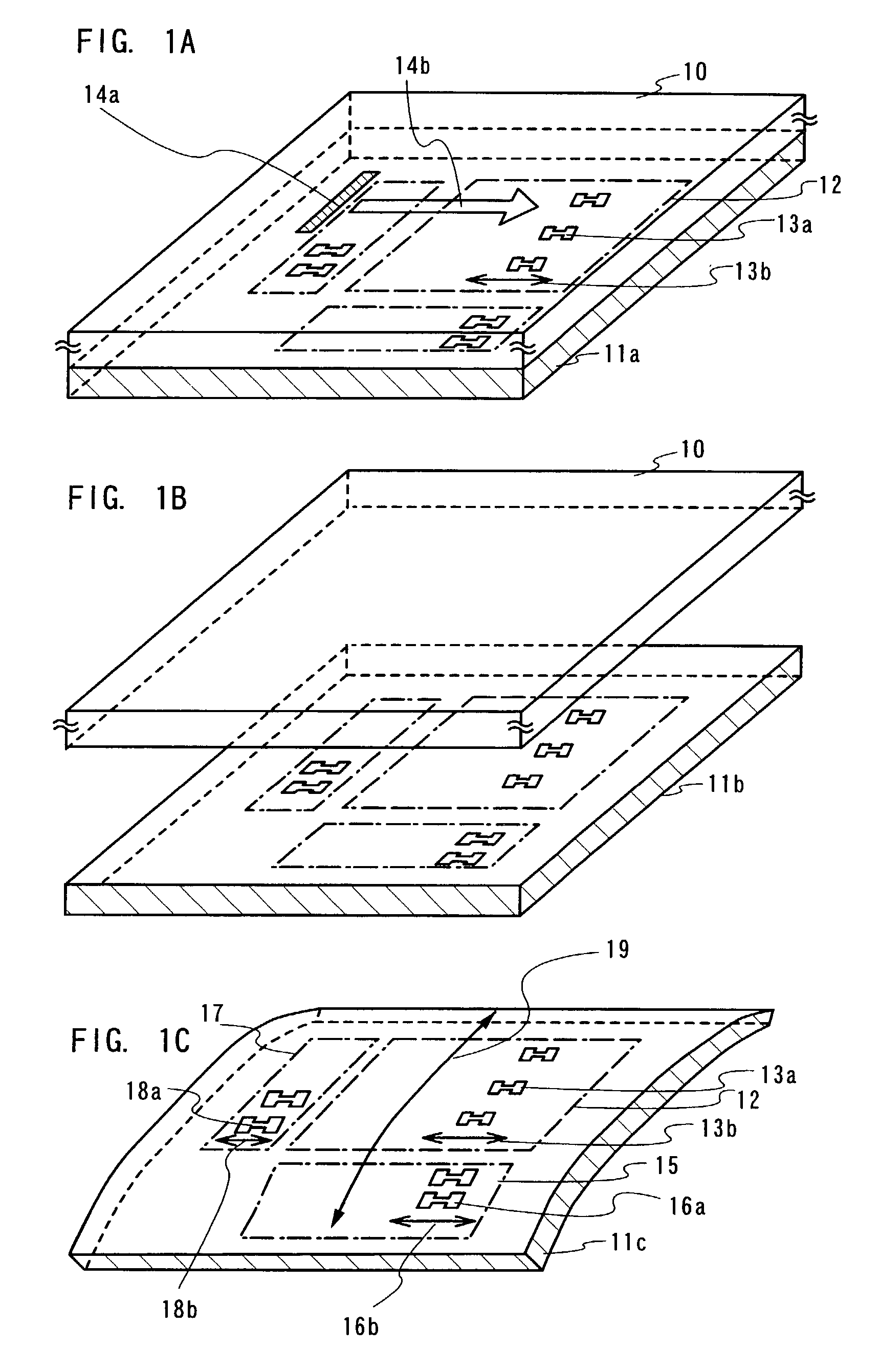
[0128]The example of the top gate TFT is described in Embodiment 1. Here, an example of a bottom gate TFT will be described. Also, the structure except for the TFT is the same one as Embodiment 1 and the description is thereof omitted here.

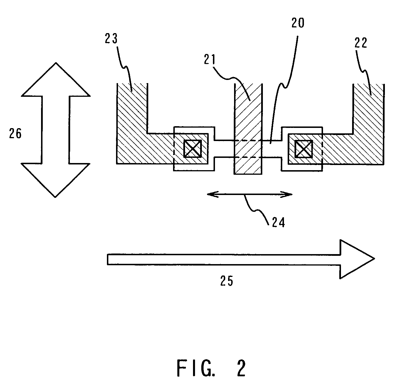
[0129]Next, steps of crystallizing a non-single crystalline semiconductor film and producing a TFT from the formed crystalline semiconductor film will be described with reference to FIGS. 7A to 7D.

[0130]FIG. 7B is a longitudinal cross sectional view. A non-single crystalline semiconductor film 503 is formed on a gate insulating film 506 covering a gate electrode. A typical example of the non-single crystalline semiconductor film 503 is an amorphous silicon film. In addition, an amorphous silicon germanium film or the like can be applied. The thickness of 10 nm to 200 nm can be applied and may be further increased in accordance with a wavelength of a laser beam and an energy density thereof. In addition, it is desirable to employ such a measure tha...

embodiment 3

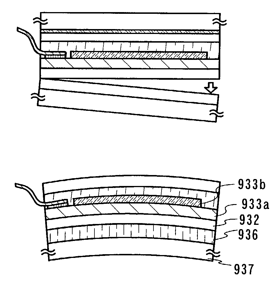
[0142]In accordance with the present embodiment, FIG. 8 shows a technique for transferring a layer to be peeled containing TFT.

[0143]In FIGS. 8A to 8G, reference numeral 830 indicates a first substrate; reference numeral 831 indicates a first material layer composed of a nitride layer or a metallic layer; reference numeral 832 indicates a second material layer composed of an oxide layer; reference numeral 833 indicates a layer to be peeled; reference numeral 834 indicates a first adhesive; reference numeral 835 indicates a second substrate; reference numeral 836 indicates a second adhesive; and reference numeral 837 indicates a third substrate.

[0144]In accordance with the present embodiment, the first substrate 830 may be constituted by a glass substrate, a quartz substrate, a ceramic substrate or the like. Further, it is also possible to use a semiconductor substrate such as a silicon substrate, or a metallic substrate such as a stainless steel substrate. Here, a glass substrate (#...


PUM


Abstract

To provide a semiconductor device in which a layer to be peeled is attached to a base having a curved surface, and a method of manufacturing the same, and more particularly, a display having a curved surface, and more specifically a light-emitting device having a light emitting element attached to a base with a curved surface. A layer to be peeled, which contains a light emitting element furnished to a substrate using a laminate of a first material layer which is a metallic layer or nitride layer, and a second material layer which is an oxide layer, is transferred onto a film, and then the film and the layer to be peeled are curved, to thereby produce a display having a curved surface.

Description

BACKGROUND OF THE INVENTION[0001]1. Field of the Invention[0002]The present invention relates to a semiconductor device having a circuit composed of thin film transistors (hereinafter referred to as TFTs) transferred by bonding a layer to be peeled off to a base member. More particularly, the present invention relates to an electro-optical device which is represented by a liquid crystal module, a light emitting device which is represented by an EL module, and electronic equipment on which such a device is mounted as a part. Further, the present invention relates to a manufacturing method of all these devices and apparatuses mentioned above.[0003]Note that a semiconductor device in this specification indicates general devices functioning by utilizing semiconductor characteristics, and an electro-optical device, a light emitting device, a semiconductor circuit, and electronic equipment are all semiconductor devices.[0004]2. Description of the Related Art[0005]In recent years, a techni...

Claims


Application Information

Patent Timeline
Patent Type & Authority Patents(United States)
IPC IPC(8): H01L21/30H01L23/50H01L21/762H01L27/32
CPCB60R11/0229B60R11/04H01L21/76251B60R1/00B60R2300/202H01L27/3244B60R2300/802B60R2011/004Y02E10/549Y02P70/50H10K59/12H10K77/111H10K59/1201H10K71/80H01L21/6835H01L27/1218H01L27/1266H01L2221/68318H01L2221/6835H01L2221/68363H01L2221/68386
Inventor TAKAYAMA, TORUMARUYAMA, JUNYAGOTO, YUUGOKUWABARA, HIDEAKIYAMAZAKI, SHUNPEI
Owner SEMICON ENERGY LAB CO LTD
Why Eureka
Try Eureka