Light-Emitting Element, Light-Emitting Device, Electronic Appliance, and Lighting Device

a technology of light-emitting devices and light-emitting elements, which is applied in the direction of solid-state devices, thermoelectric devices, organic chemistry, etc., can solve the problems of difficult to obtain features, and achieve the effects of low driving voltage, low power consumption, and high current efficiency

Inactive Publication Date: 2014-07-03
SEMICON ENERGY LAB CO LTD
View PDF2 Cites 389 Cited by
  • Summary
  • Abstract
  • Description
  • Claims
  • Application Information

AI Technical Summary

Benefits of technology

[0023]According to one embodiment of the present invention, a light-emitting element which has low driving voltage and high current efficiency can be provided. According to one embodiment of the present invention, the use of the light-emitting element makes it possible to provide a light-emitting device, an electronic device, and a lighting device which have lower power consumption.

Problems solved by technology

This feature is difficult to obtain with point light sources typified by incandescent lamps and LEDs or linear light sources typified by fluorescent lamps.

Method used


Image

  • Light-Emitting Element, Light-Emitting Device, Electronic Appliance, and Lighting Device
  • Light-Emitting Element, Light-Emitting Device, Electronic Appliance, and Lighting Device
  • Light-Emitting Element, Light-Emitting Device, Electronic Appliance, and Lighting Device

Examples


embodiment 1

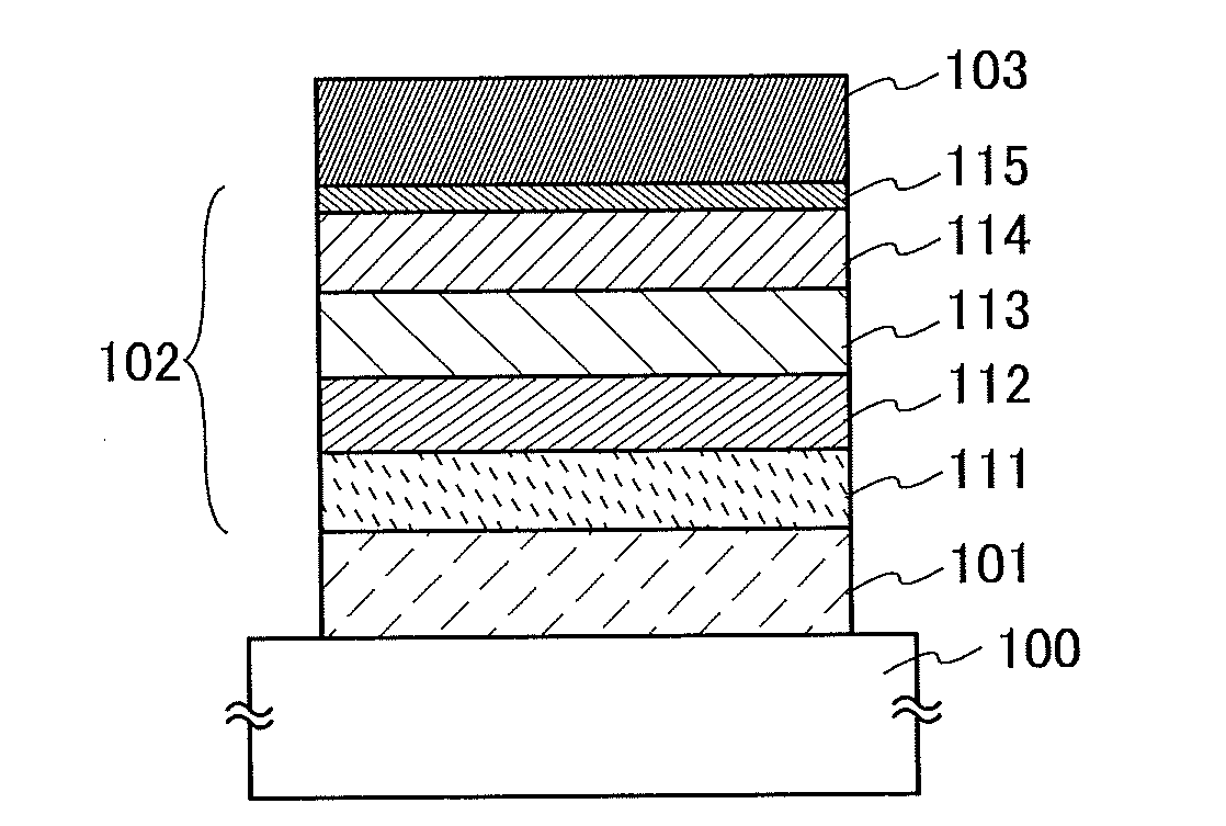
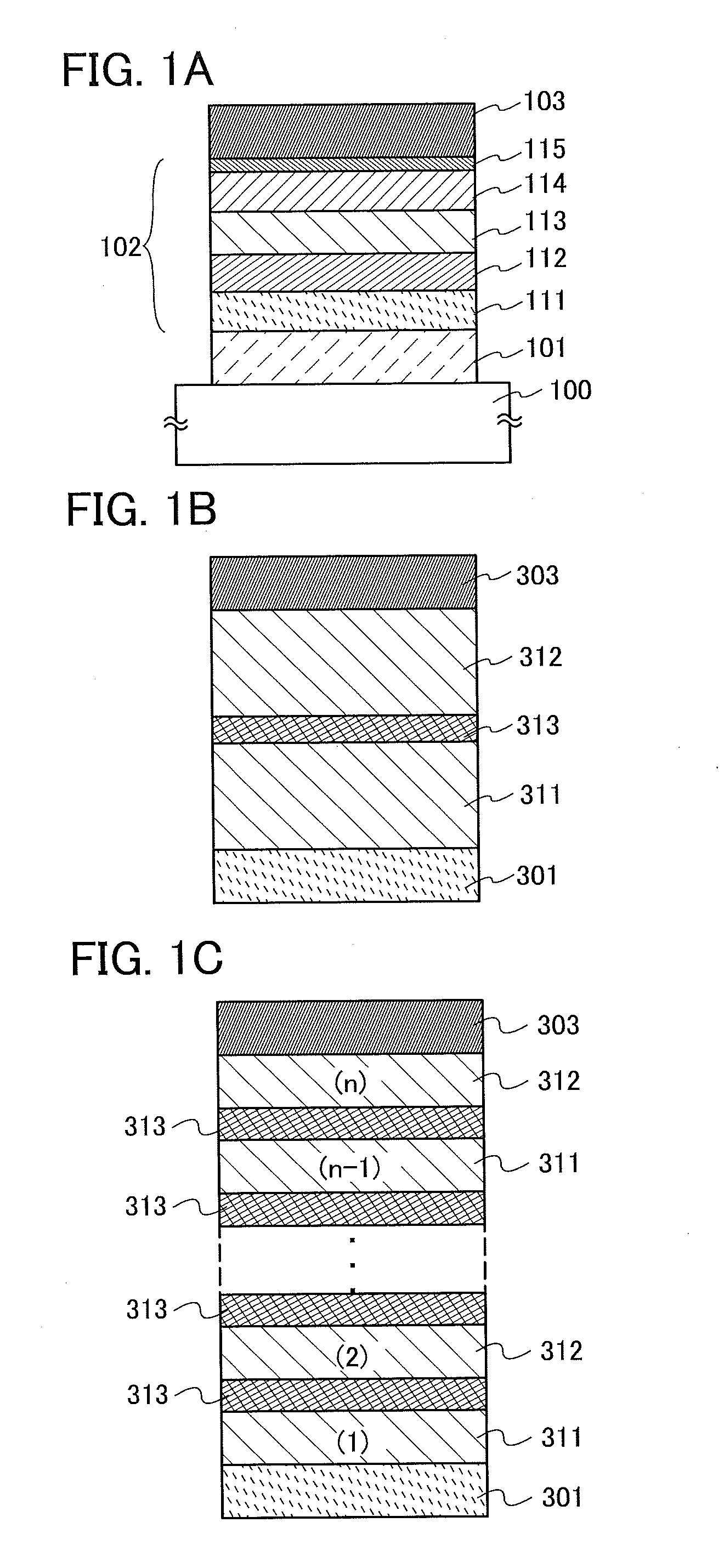
[0061]In this embodiment, light-emitting elements each of which includes a light-emitting layer between a pair of electrodes are described with reference to FIGS. 1A to 1C.

[0062]First, the light-emitting element illustrated in FIG. 1A is described.

[0063]As illustrated in FIG. 1A, the light-emitting element described in this embodiment includes an EL layer 102 between a first electrode 101 and a second electrode 103. The EL layer 102 includes at least a light-emitting layer 113 and also includes a hole-injection layer 111, a hole-transport layer 112, an electron-transport layer 114, an electron-injection layer 115, and the like. Note that in this embodiment, the first electrode 101 is used as an anode and the second electrode 103 is used as a cathode.

[0064]The light-emitting layer 113 contains an organic compound. The organic compound has a dibenzo[f,h]quinoline ring, an arylene group, and a hole-transport skeleton. It is particularly preferable that the dibenzo[f,h]quinoline ring an...

embodiment 2

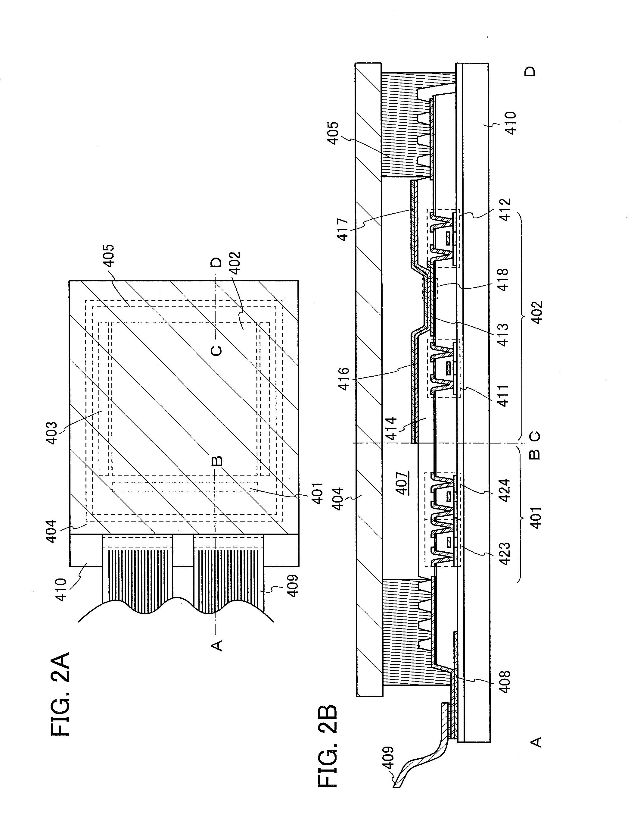
[0149]In this embodiment, a light-emitting device which includes the light-emitting element of one embodiment of the present invention will be described with reference to FIGS. 2A and 2B. Note that FIG. 2A is a top view illustrating the light-emitting device, and FIG. 2B is a cross-sectional view taken along the lines A-B and C-D in FIG. 2A.

[0150]The light-emitting device of this embodiment includes a source side driver circuit 401 and a gate side driver circuit 403 which are driver circuit portions, a pixel portion 402, a sealing substrate 404, a sealant 405, a flexible printed circuit (FPC) 409, and an element substrate 410. A portion enclosed by the sealant 405 is a space 407.

[0151]Note that a lead wiring 408 is a wiring for transmitting signals that are to be input to the source side driver circuit 401 and the gate side driver circuit 403, and receives a video signal, a clock signal, a start signal, a reset signal, and the like from an FPC 409 which serves as an external input t...

embodiment 3

[0165]In this embodiment, a light-emitting device manufactured using the light-emitting element of one embodiment of the present invention is described with reference to FIGS. 4A and 4B.

[0166]In FIG. 4A, a plan view of a light-emitting device described in this embodiment and a cross-sectional view taken along dashed-dotted line E-F in the plan view are illustrated.

[0167]The light-emitting device illustrated in FIG. 4A includes a light-emitting portion 2002 including a light-emitting element over a first substrate 2001. The light-emitting device has a structure in which a first sealant 2005a is provided so as to surround the light-emitting portion 2002 and a second sealant 2005b is provided so as to surround the first sealant 2005a (i.e., a double sealing structure).

[0168]Thus, the light-emitting portion 2002 is positioned in a space surrounded by the first substrate 2001, the second substrate 2006, and the first sealant 2005a.

[0169]Note that in this specification, the first sealant...


PUM


Abstract

Disclosed is a light-emitting element having high emission efficiency, capable of driving at low voltage, and showing a long lifetime. The light-emitting element contains a compound between a pair of electrodes, and the compound is configured to give a first peak of m/z around 202 and a second peak of m/z around 227 in a mass spectrum. The first and second peaks are product ions of the compound and possess compositions of C16H9 and C17H10N, respectively, which are derived from a dibenzo[f,h]quinoline unit.

Description

BACKGROUND OF THE INVENTION[0001]1. Field of the Invention[0002]One embodiment of the present invention relates to, for example, a light-emitting element containing an organic compound that is capable of converting triplet excited energy into luminescence. One embodiment of the present invention also relates to, for example, a light-emitting device, an electronic appliance, and a lighting device each of which includes the light-emitting element.[0003]2. Description of the Related Art[0004]In recent years, research and development have been actively conducted on light-emitting elements using electroluminescence (EL). In a basic structure of such a light-emitting element, a layer containing a light-emitting substance is interposed between a pair of electrodes. By applying voltage to this element, light emission from the light-emitting substance can be obtained.[0005]Such a light-emitting element is self-luminous elements and has advantages over liquid crystal displays, such as high vi...

Claims


Application Information

Patent Timeline
Patent Type & Authority Applications(United States)
IPC IPC(8): H01L51/00
CPCH01L51/0074H01L51/0072C07D401/10C07D405/10C07D409/10H10K85/6572H10K50/11H10K2101/10H10K2101/00H10K85/6576
Inventor KADOMA, HIROSHIOGITA, KAORISHITAGAKI, SATOKOOHSAWA, NOBUHARUSEO, SATOSHIOSAKA, HARUE
Owner SEMICON ENERGY LAB CO LTD
Why Eureka
Try Eureka