Homoepitaxial gallium-nitride-based light emitting device and method for producing

a light emitting device and gallium nitride technology, applied in the field of light applications, can solve the problems of poor thermal conductivity of sapphire, inability to manufacture high-quality gan substrates, and limited use of sapphire substrates with a low-temperature buffer layer

Inactive Publication Date: 2006-05-30
SLT TECH +1
View PDF14 Cites 394 Cited by
  • Summary
  • Abstract
  • Description
  • Claims
  • Application Information

AI Technical Summary

Benefits of technology

[0023]In an exemplary embodiment of the present invention, a light emitting device comprised of a light emitting semiconductor active region disposed on a substrate comprised of GaN that is substantially free of tilt boundaries and having a dislocation density less than 104 per cm2, more preferably below 103 per cm2, and, even more preferably, below 100 per cm2, is provided.
[0024]In a further exemplary embodiment of the present invention, a method for the preparation of a light emitting device comprising disposing a group III semiconductor active region on a substrate comprised of GaN that is substantially free of tilt boundaries in the absence of low-temperature buffer layers is described.
[0025]In yet another exemplary embodiment of the present invention, a homoepitaxial light emitting diode is provided. The homoepitaxial light emitting diode is comprised of: a n-electrode, a n-GaN substrate that is substantially free of tilt boundaries; optionally, at least one n-GaN or n-AluInvGa1-u-vN cladding layer, an AlwInxGa1-w-xN active layer, at least one p-AlyInzGa1-y-zN cladding layer or p-GaN cladding layer; and a p-electrode, wherein 0≦u, v, w, x, y, z≦1, 0≦u+v, w+x, y+Z≦1, and wherein the band gap of the active layer is less than the band gap of the cladding layers.
[0026]In an additional exemplary embodiment of the present invention, a homoepitaxial laser diode is provided. The homoepitaxial laser diode comprises: a n-electrode; a n-GaN substrate that is substantially free of tilt boundaries; at least one n-GaN or n-AlaInbGa1-a-bN cladding layer; optionally, at least one n-AlcIndGa1-c-dN optical guiding layer; a AleInfGa1-e-fN / AlgInhGa1-g-hN multiple quantum well; optionally, a p-AliInjGa1-i-jN blocking layer; optionally, as least one p-AlkInlGa1-k-lN optical guilding layer; at least one p-AlmInnGa1-m-n1N cladding layer; optionally, a p-AloInpGa1-o-pN contact layer; and a p-electrode, wherein 0≦a, b, c, d, e, f g, h, i, j, k, l, m, n, o, p≦1, 0≦a+b, c+d, e+f, g+h, i+j, k+l, m+n, o+p≦1, wherein the band gap of the multiple quantum well active layer is less than that of the optical guiding layers, which are in turn less than that of the cladding layers, which are less than that of the p-type blocking layer. Sidewalls and parallel facets are then provided in directions perpendicular to the deposited layers.

Problems solved by technology

Because high-quality GaN substrates have not been available, virtually all of the art has involved heteroepitaxial deposition of GaN and GaInAlN on sapphire or SiC substrates.
The use of sapphire substrates with a low-temperature buffer layer has a number of important limitations for manufacture of LEDs.
In addition, sapphire has a rather poor thermal conductivity, limiting heat dissipation.
These dislocations can act as non-radiative recombination centers and may limit performance in certain applications, such as, for example, reducing emission efficiency in near-ultraviolet and high power LEDs and LDs and reducing the lifetime in LDs.
Deposition of the low-temperature buffer layer also adds cost and complexity to the process.
Sapphire also has a large (45%) mismatch in the thermal expansion coefficient with respect to GaN, which generates stresses in device structures upon cooldown from the processing temperature and limits the maximum size of wafers and thickness of epitaxial layers that can be used without forming cracks.
Facets must be prepared at the ends of laser diode structures in order to define the laser cavity, and the difficulty in cleaving c-axis-oriented sapphire makes facet preparation more expensive.
The use of SiC substrates alleviates some of these limitations but introduces other problems.
The SiC lattice mismatch to GaN is smaller than that of sapphire, but very high defect concentrations are still generated, and the use of low-temperature buffer films is still needed.
SiC is also much more expensive than sapphire.
Lower cost SiC is typically opaque, decreasing the efficiency of the LED device because light emitted from the active region toward the substrate would be absorbed rather than transmitted.
Some limited work has previously been carried out on forming homoepitaxial LED or LD devices on GaN substrates.
Therefore, the devices demonstrated by Pelzmann, et al. do not offer any performance advantages relative to conventional heteroepitaxial LEDs.
rate. This constitutes a large disadvantage compared to conventional heteroepitaxial LEDs fabricated on sapphire or transparent SiC subst
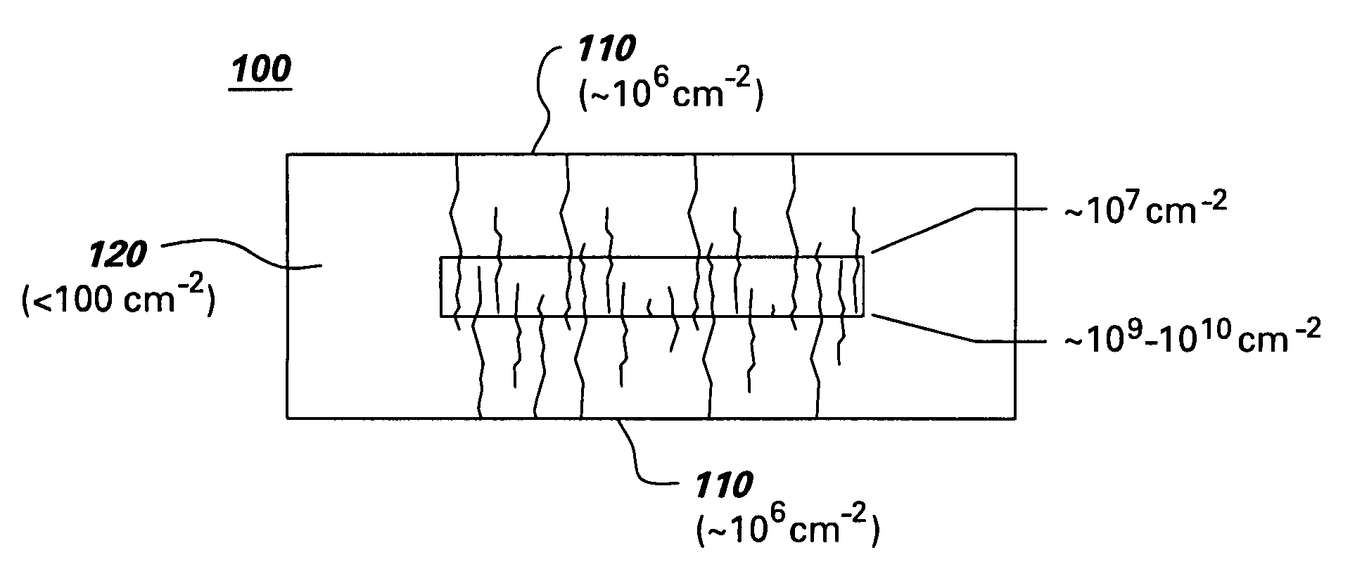
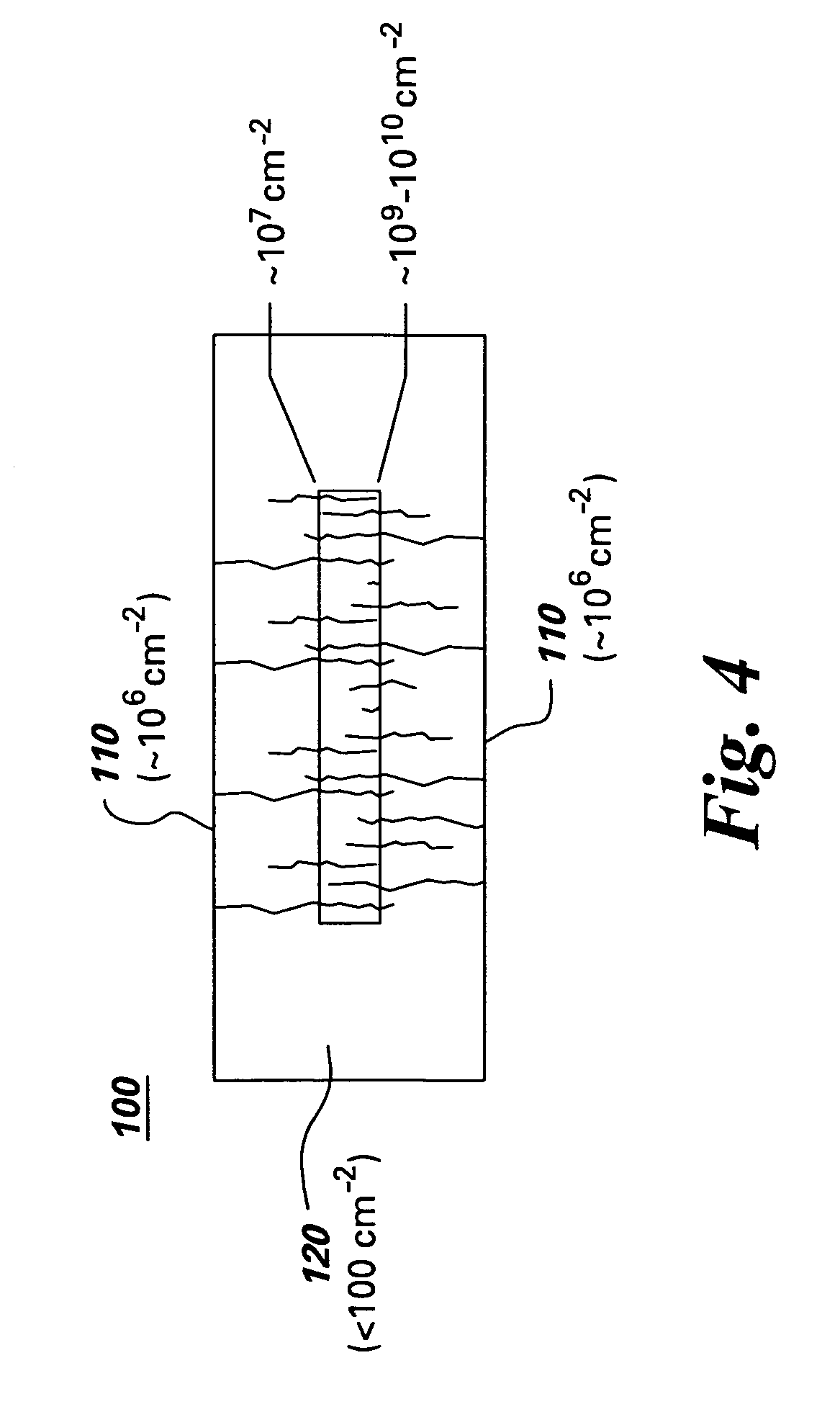
2. This value is lower than the corresponding values in heteroepitaxial LEDs of approximately 107 to 1010 cm−2 but will still result in dislocations being present in large-area
thereupon. Additionally, the undoped GaN substrates employed by Kamp et al. have a rather limited carrier mobility, about 30–90 cm2 / V-s, which may be limiting in high-po
However, these crystals are semi-insulating, with an electrical resistivity of 104–106 Ω-cm at room temperature, rendering them unsuitable as substrates for vertical light-emitting structures of one type described in the present invention.
These substrates have several additional disadvantages, including: (i) a high concentration (approximately 1019 cm−1) of Mg and O atoms, each [J. I. Pankove et al., Appl. Phys. Lett. 74, 416 (1999)], which could potentially diffuse into device structures during high temperature processing; and (ii) relatively poor thermal conductivity.
A final but very important limitation of the method of Porowski et al. is that it does not appear to be scalable; that is, the method is incapable of producing GaN boules and wafers having diameters greater than or equal to 50 mm.
Because the process of Porowski et al. yields platelets rather than thick boules, the economies of scale associated with conventional wafering technology (slicing, polishing) cannot be achieved.
In addition, strain is present in HVPE wafers due to the thermal expansion mismatch between substrate and film.
This behavior will compromise the performance of light emitting devices operating in the ultraviolet, as some of the light will be absorbed by the substrate rather than being emitted.
However, light emitting devices fabricated on ELO substrates typically have a surface area of at least about 104 μm2 (10−4 cm2) and still contain a substantial number of threading dislocations.
In addition, the GaN substrate is likely to suffer from the same deficiencies in UV absorption and photoluminescence at room temperature as “standard” HVPE GaN.
Residual stress or strain in homoepitaxial GaN-based devices resulting, for example, from the presence of tilt boundaries, may accelerate the degradation of LDs or high-power LEDs.
Similarly, dislocations associated with tilt boundaries may reduce the lifetime of high-power light emitting diodes and laser diodes.
Dislocations may also increase reverse-bias current leakage, further degrading device performance.
Clearly, the presence of even a single dislocation within a GaN-based light-emitting device can degrade its performance and / or lifetime.
Gallium nitride grown by all known methods contains native defects that may degrade the properties of the crystal and of devices grown thereupon.
However, known GaN crystal growth methods do not provide a means for passivating Ga vacancies by hydrogenation.
As with other ELO methods, coalescence of laterally-grown GaN will cause formation of tilt boundaries in these base layers.

Method used


Image

  • Homoepitaxial gallium-nitride-based light emitting device and method for producing
  • Homoepitaxial gallium-nitride-based light emitting device and method for producing
  • Homoepitaxial gallium-nitride-based light emitting device and method for producing

Examples


Embodiment Construction

[0035]The present invention describes a homoepitaxial light emitting device and a method for forming that device. The present inventive device is a GaN based LED or LD grown on a GaN substrate that is substantially free of tilt boundaries. The LED or LD devices of the present invention are referred to as homoepitaxial even though the composition (AluInvGa1-u-vN) and lattice constants of the active and cladding layers are not identical to those of the substrate (GaN), because the lattice constants of the active and cladding layers are typically close to those of GaN and the underlying chemistry is very similar, as all of the layers comprise at least one group III nitride. The GaN substrate for the device fabrication consists of a GaN wafer cut from a boule that was grown using a supercritical solvent at a temperature greater than about 550° C. and a pressure greater than about 5 kbar. In one embodiment, the substrate has a (0001) orientation. In other embodiments, the orientation may...


PUM


Abstract

A light emitting device, such as a light emitting diode or a laser diode. The light emitting device comprises a light emitting semiconductor active region disposed on a substrate. The substrate comprises an optical absorption coefficient below about 100 cm−1 at wavelengths between 700 and 465 nm a GaN single crystal having a dislocation density of less than 104 per cm2 and an optical absorption coefficient below about 100 cm−1 at wavelengths between 700 and 465 nm. A method of making such a light emitting device is also provided.

Description

CROSS REFERENCE TO RELATED APPLICATION[0001]This application is a continuation-in-part of application Ser. No. 10 / 440,574, filed May 19, 2003, which is a Division of application Ser. No. 09 / 694,690, filed Oct. 23, 2000, and claims benefit therefrom.BACKGROUND OF THE INVENTION[0002]The present invention relates to lighting applications, more specifically to light emitting diode (LED) and laser diode (LD) applications. More specifically, the present invention relates to a homoepitaxial LED or LD structure and a method for making such a structure.[0003]During the past decade there has been tremendous interest in gallium nitride (GaN) based optoelectronic devices, including light emitting diodes and laser diodes. Because high-quality GaN substrates have not been available, virtually all of the art has involved heteroepitaxial deposition of GaN and GaInAlN on sapphire or SiC substrates. A thin low-temperature buffer layer, typically AlN or GaN, is used in order to accommodate the lattice...

Claims


Application Information

Patent Timeline
Patent Type & Authority Patents(United States)
IPC IPC(8): H01L27/15H01L33/32
CPCH01L33/32
Inventor D'EVELYN, MARK PHILIPEVERS, NICOLE ANDREALEBOEUF, STEVEN FRANCISCAO, XIAN-ANZHANG, AN-PING
Owner SLT TECH
Why Eureka
Try Eureka