Touch panel device

a technology of touch panel and device, which is applied in the direction of piezoelectric/electrostrictive/magnetostrictive devices, piezoelectric/electrostriction/magnetostriction machines, instruments, etc., can solve the problems of reducing yield, increasing manufacturing costs, and affecting the efficiency of propaga

Inactive Publication Date: 2005-06-28
FUJITSU LTD
View PDF10 Cites 18 Cited by
  • Summary
  • Abstract
  • Description
  • Claims
  • Application Information

AI Technical Summary

Benefits of technology

[0021]According to each structure of the present invention, due to a difference of propagation speed of the surface acoustic wave between the area with the piezoelectric thin film and the area without the piezoelectric thin film (i.e., the touch area), the surface acoustic wave emitted from the comb electrode of the transmission element is first refracted in a certain direction at the boundary of the piezoelectric thin film and the touch area and is refracted again when entering the piezoelectric thin film of the reception element side from the touch area, so as to enter the comb electrode of the reception element perpendicularly. Thus, the surface acoustic wave can propagate efficiently from the transmission element to the reception element.

Problems solved by technology

However, the structure shown in FIG. 10 has a disadvantage.
As a result, yield may drop and manufacturing cost may increase.

Method used


Image

  • Touch panel device
  • Touch panel device
  • Touch panel device

Examples


Embodiment Construction

[0033]Hereinafter, the present invention will be explained more in detail with reference to embodiments and drawings.

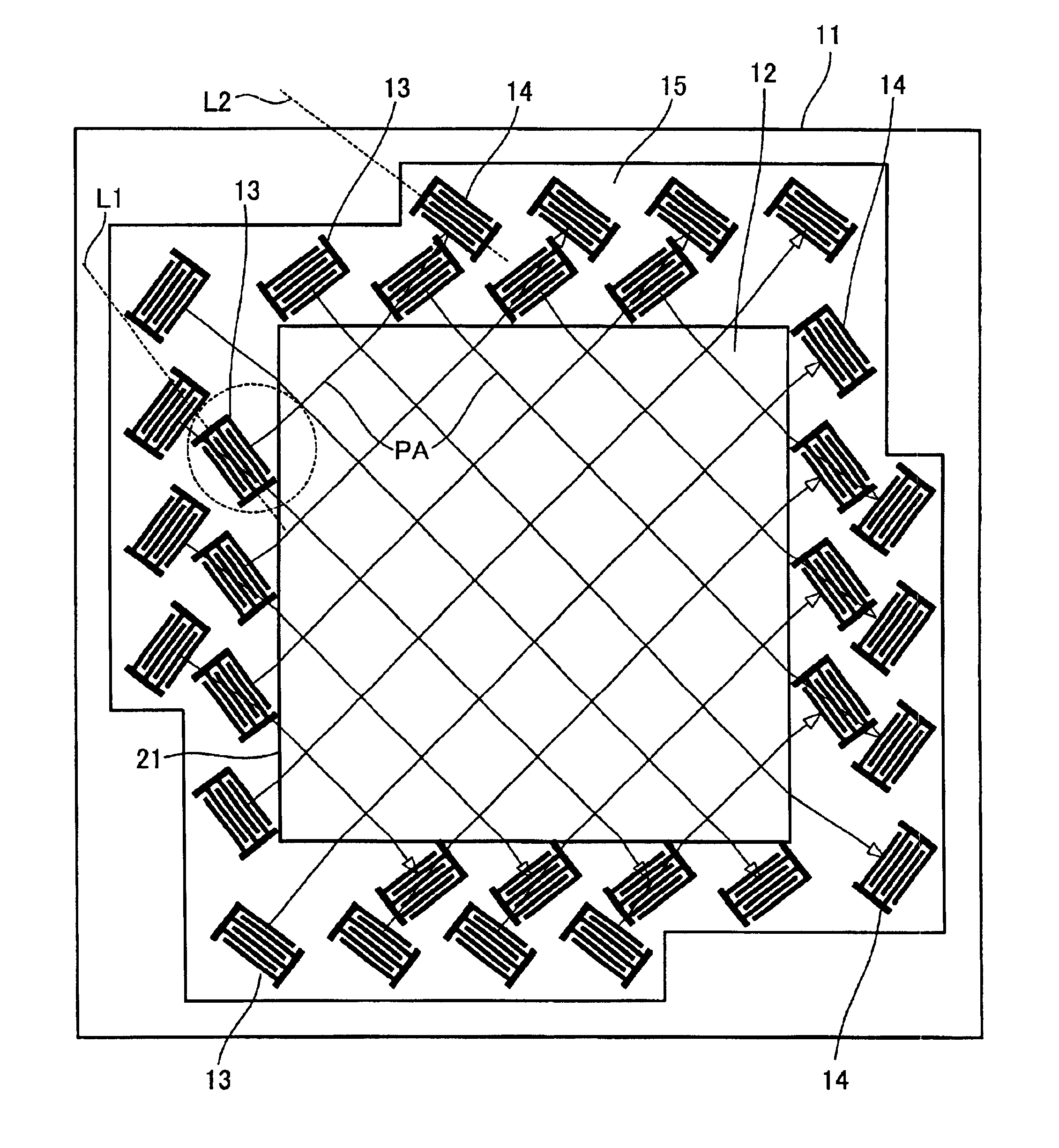
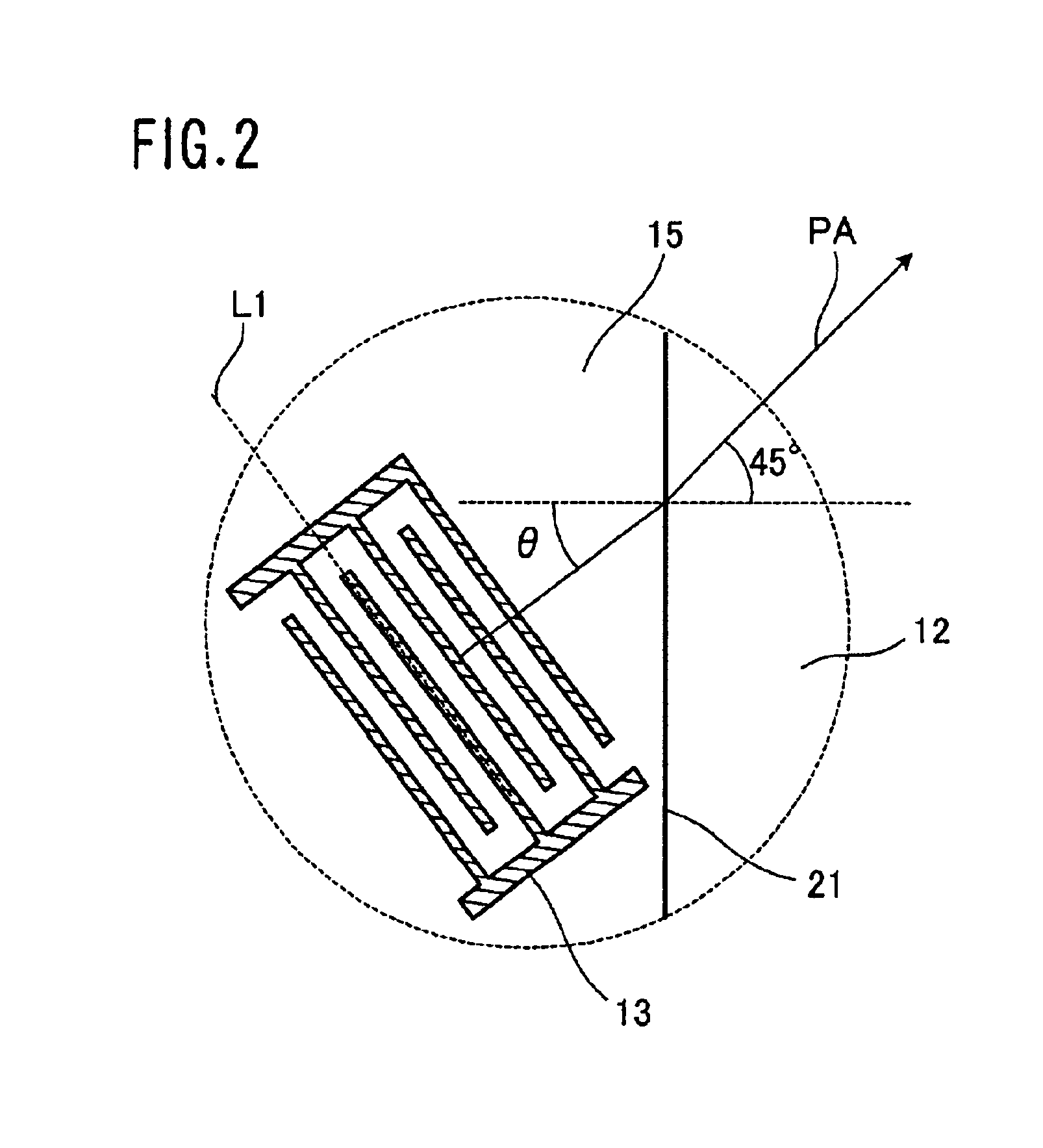
[0034]FIG. 1 shows a simplified structure of a touch panel device including a touch area and the periphery thereof according to a first embodiment of the present invention. On the middle portion of a glass substrate 11, a rectangular touch area 12 is provided, and plural pairs of comb electrodes 13 and 14 are arranged around the touch area 12. The comb electrode 13 makes up a SAW transmission element, while the comb electrode 14 makes up a SAW reception element.

[0035]Surface acoustic wave signals propagate in a slanting direction from the transmission comb electrodes 13 arranged along one side of the touch area 12 to the reception comb electrodes 14 arranged along the neighboring side, as shown by lines with arrows. In order to simplify the explanation, it is supposed that the touch area 12 is square, and the propagation paths (lines with arrows) PA of the surface aco...


PUM


Abstract

A touch panel device is provided that can detect a touched position with sufficient resolution and accuracy without requiring high accuracy in process for forming a piezoelectric thin film. In the middle portion of the glass substrate, a substantially rectangular touch area is provided. In the periphery of the touch area, plural transmission comb electrodes arranged along one of the neighboring sides of the touch area and plural reception comb electrodes arranged along the other of the neighboring sides make pairs. Surface acoustic wave signals propagate from the transmission comb electrodes to the reception comb electrodes in a slanting direction with respect to four sides of the touch area. The inside edge of the piezoelectric thin film is formed linearly along the sides of the touch area. Each of the comb electrodes 13 and 14 are arranged so that the line along the electrode finger of the transmission comb electrode and the line along the electrode finger of the reception comb electrode are non-parallel with each other in accordance with an angle of refraction of the surface acoustic wave at the boundary between the piezoelectric thin film and the touch area.

Description

BACKGROUND OF THE INVENTION[0001]1. Field of the Invention[0002]The present invention relates to a touch panel device that can be used as an input device for equipment such as a personal computer. More specifically, the present invention relates to a touch panel device having plural pairs of surface acoustic wave transmission elements and reception elements, each of which includes a comb electrode and a piezoelectric thin film, for detecting a touched position.[0003]2. Description of the Prior Art[0004]Such a touch panel device can provide a user-friendly input interface being combined with a display device such as a CRT or an LCD. For example, a command input or selection can be performed easily by touching a button or an icon displayed on a screen of the display device.[0005]FIG. 9 shows a simplified structure of a conventional touch panel device utilizing a surface acoustic wave (also referred to as “SAW”). On the middle portion of a substrate 51 such as a glass plate, a rectangu...

Claims


Application Information

Patent Timeline
Patent Type & Authority Patents(United States)
IPC IPC(8): G06F3/033G06F3/043G06F3/041
CPCG06F3/0436
Inventor KATSUKI, TAKASHINAKAZAWA, FUMIHIKOSANO, SATOSHITAKAHASHI, YUJI
Owner FUJITSU LTD
Why Eureka
Try Eureka