Semiconductor package and method of fabricating same

a technology of semiconductor packaging and semiconductor components, which is applied in the direction of semiconductor devices, semiconductor/solid-state device details, electrical apparatus, etc., can solve the problems of increasing manufacturing costs, reducing the quantity of output, and increasing the whole manufacturing time of semiconductor packages, so as to reduce packaging time and stabilize the product structure

Inactive Publication Date: 2005-07-26
SHEN YU NUNG
View PDF6 Cites 10 Cited by
  • Summary
  • Abstract
  • Description
  • Claims
  • Application Information

AI Technical Summary

Benefits of technology

[0007]It is therefore a principal object of the present invention to provide a semiconductor package and a method of fabricating a semiconductor package, which can reduce packaging time and obtain steadier product structure. Furthermore, the present invention has been accomplished to eliminate the aforesaid problem.

Problems solved by technology

However, in the formation of the solder ball on the bonding pad of the semiconductor die as described above, the reflow process is lengthy, causing the whole manufacturing time of the semiconductor package to increase, and thus the quantity of output is reduced and the manufacturing cost is increased.
Thus, it is easy to generate poor contact or no connection when the semiconductor package is electrically connected to an external circuit.

Method used


Image

  • Semiconductor package and method of fabricating same
  • Semiconductor package and method of fabricating same
  • Semiconductor package and method of fabricating same

Examples


first embodiment

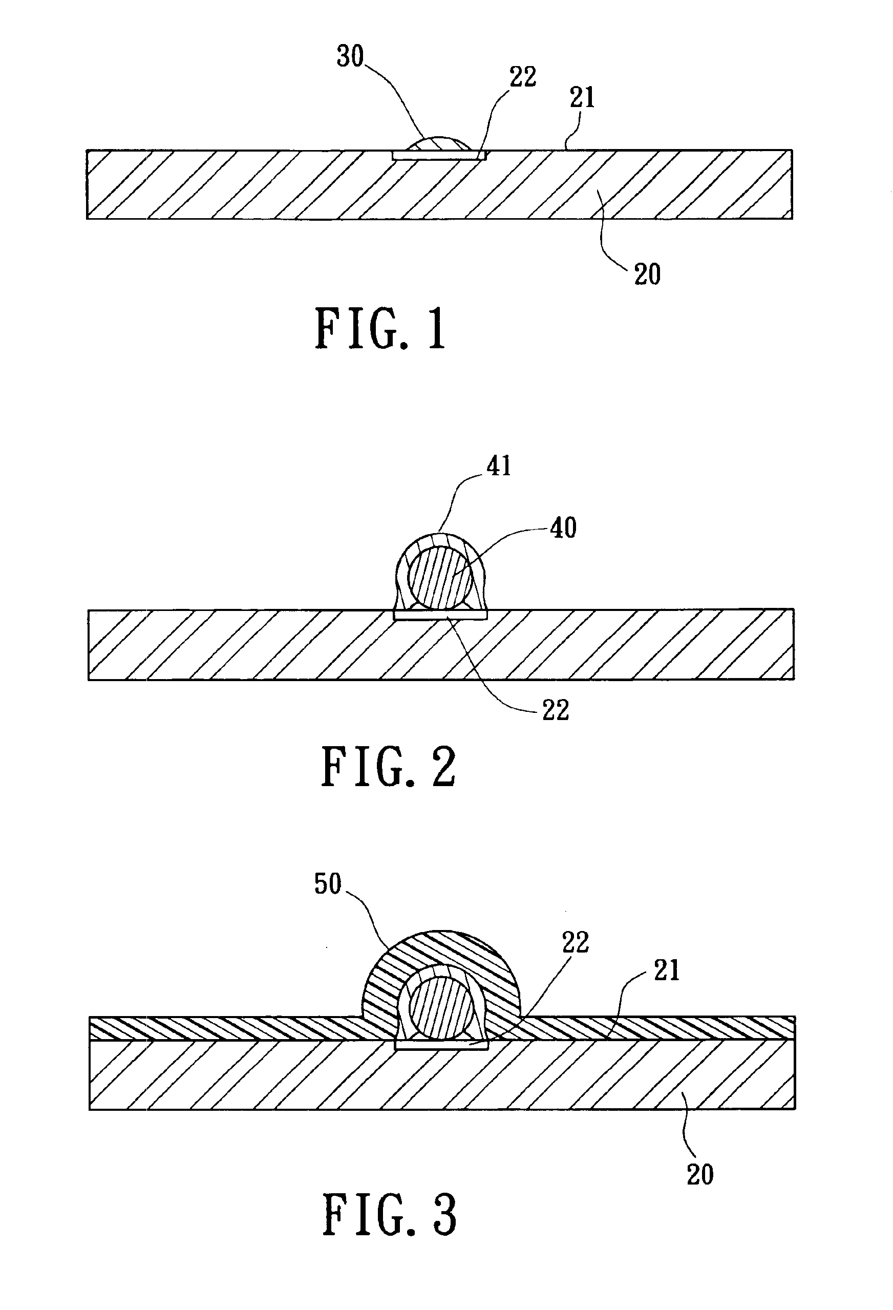
[0017]Reference is now made to the drawings, which are for the purpose of illustrating preferred embodiments of the present invention, only, and not for the purpose of limiting the same. FIGS. 1-4 are cross-sectional views illustrating a sequence of steps for manufacturing the semiconductor package in accordance with the present invention.

[0018]First, as shown in FIG. 1, a semiconductor die 20 having a pad mounting surface 21 and a plurality of bonding pads 22 disposed on the pad mounting surface 21 (only showing single bonding pad in the drawing) is provided. A medium 30 is attached on a center portion of each of the bonding pads 22 of the semiconductor die 20 as a fastening means. The medium 30 is a conductive material or a non-conductive material.

[0019]It should be noted that the semiconductor die 20 can be an individual semiconductor die diced from a wafer, or can be one of the semiconductor dies of a wafer.

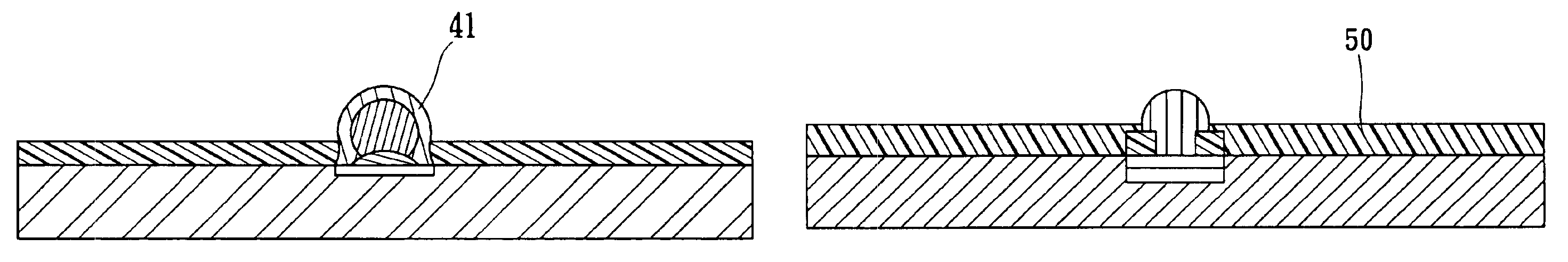
[0020]Next, a spherical element 40 is arranged on each of the bonding pa...

second embodiment

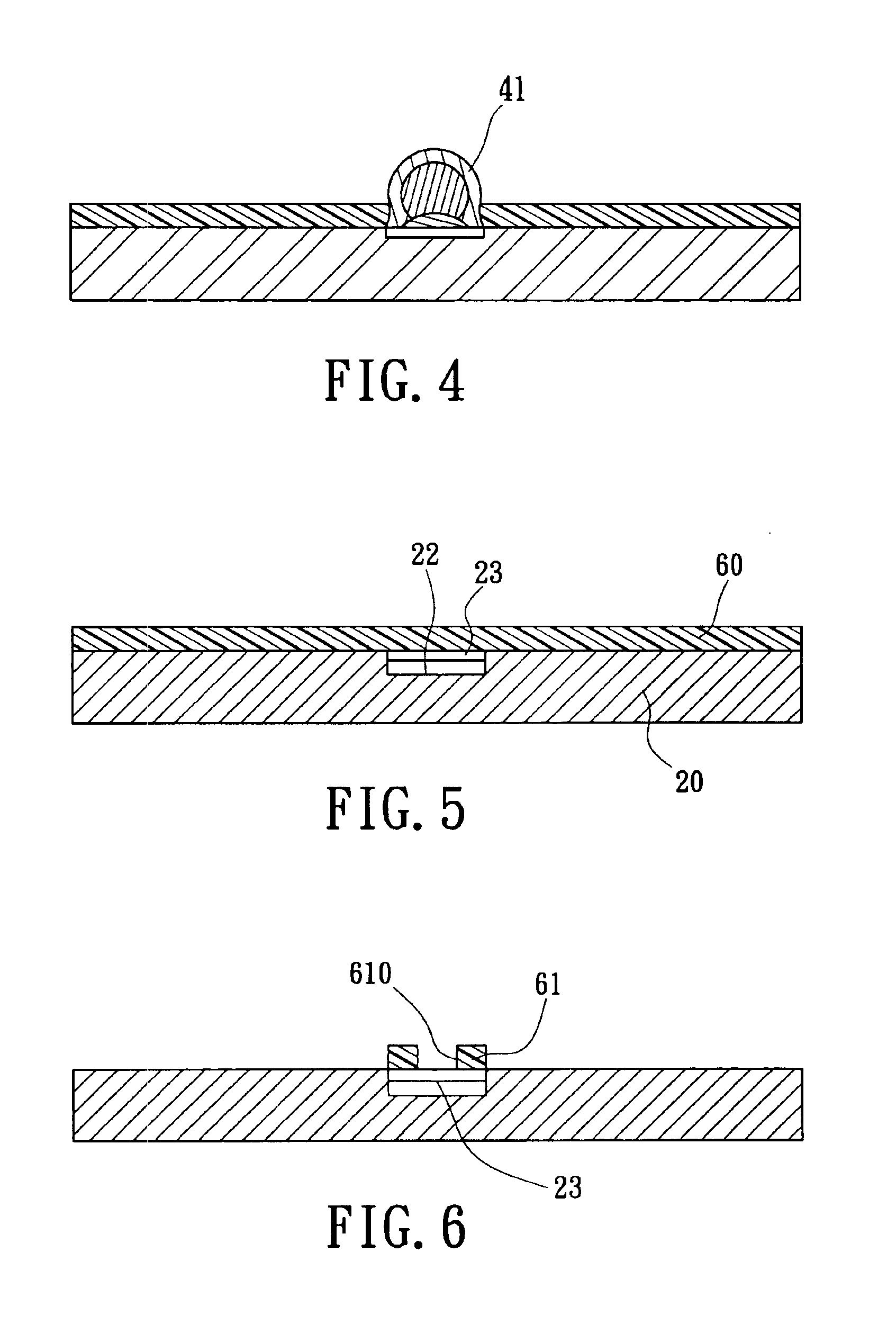
[0023]FIGS. 5-9 are cross-sectional views illustrating a sequence of steps for manufacturing the semiconductor package in accordance with the present invention.

[0024]As shown in FIG. 5, a semiconductor die 20 having a pad mounting surface 21 and a plurality of bonding pads 22 disposed on the pad mounting surface 21 (only showing single bonding pad in the drawing) is provided. A metal conductive layer 23 is formed on each of the bonding pads 22. Further, a covering layer 60 is coated on the pad mounting surface 21 of the semiconductor die 20 by means of a photoresist material.

[0025]Next, the covering layer 60 is patterned and etched so as to form a plurality of conductor holders 61 on the respective metal conductive layers 23. Each of the conductor holders 61 has an indentation 610 down to the corresponding metal conductive layer 23, as shown in FIG. 6.

[0026]Subsequently, a conductor 70, such as a solder ball is arranged in the indentation 610 of each of the conductor holders 61, as ...


PUM


Abstract

A semiconductor package and a method of fabricating a semiconductor package are provided. The method of fabricating a semiconductor package provides a semiconductor die having a pad mounting surface and a plurality of bonding pads disposed on the pad mounting surface; attaches a medium on each of the bonding pads; arranges a spherical element on each of the bonding pads via the corresponding medium; forms an electroplating layer on each of the spherical elements and around the corresponding medium; and coats a protection layer on the pad mounting surface of the semiconductor die and the electroplating layers by means of a photoresist material. Furthermore, the protection layer is patterned and etched so as to expose the top portions of the electroplating layers.

Description

BACKGROUND OF THE INVENTION[0001]1. Field of the Invention[0002]The present invention relates to a semiconductor package and, more particularly, to a semiconductor package and a method of fabricating a semiconductor package, which can reduce packaging time and provide a steadier product structure.[0003]2. Description of the Related Art[0004]The formation of a solder ball on a bonding pad of a semiconductor die will now be explained with the reference of FIGS. 10 and 11.[0005]First, as shown in FIG. 10, a semiconductor die 10 is prepared. The semiconductor die 10 has at least one bonding pad 11 on its pad mounting surface. A layer of solder paste 13 is applied on the bonding pad 11 of the semiconductor die 10. As shown in FIG. 11, a solder ball 12 is formed from the layer of solder paste 13 in a reflow process, such that a semiconductor package is constituted.[0006]However, in the formation of the solder ball on the bonding pad of the semiconductor die as described above, the reflow ...

Claims


Application Information

Patent Timeline
Patent Type & Authority Patents(United States)
IPC IPC(8): H01L21/60H01L21/02H01L23/31H01L23/485
CPCH01L23/3157H01L24/11H01L24/12H01L2924/014H01L2224/13099H01L2924/01033H01L2224/05001H01L2224/05026H01L2224/05571H01L2224/05573H01L2924/00014H01L2224/05599H01L2224/05099
Inventor SHEN, YU-NUNG
Owner SHEN YU NUNG
Why Eureka
Try Eureka