
Multi-bank memory accesses using posted writes

a multi-bank and memory access technology, applied in memory adressing/allocation/relocation, digital storage, instruments, etc., can solve the problem that the memory device cannot be modified to accommodate the adjusted relative timing, and achieve the effect of reducing the read-write access delay

Inactive Publication Date: 2005-08-30
ROUND ROCK RES LLC
View PDF15 Cites 109 Cited by
  • Summary
  • Abstract
  • Description
  • Claims
  • Application Information

AI Technical Summary

Benefits of technology

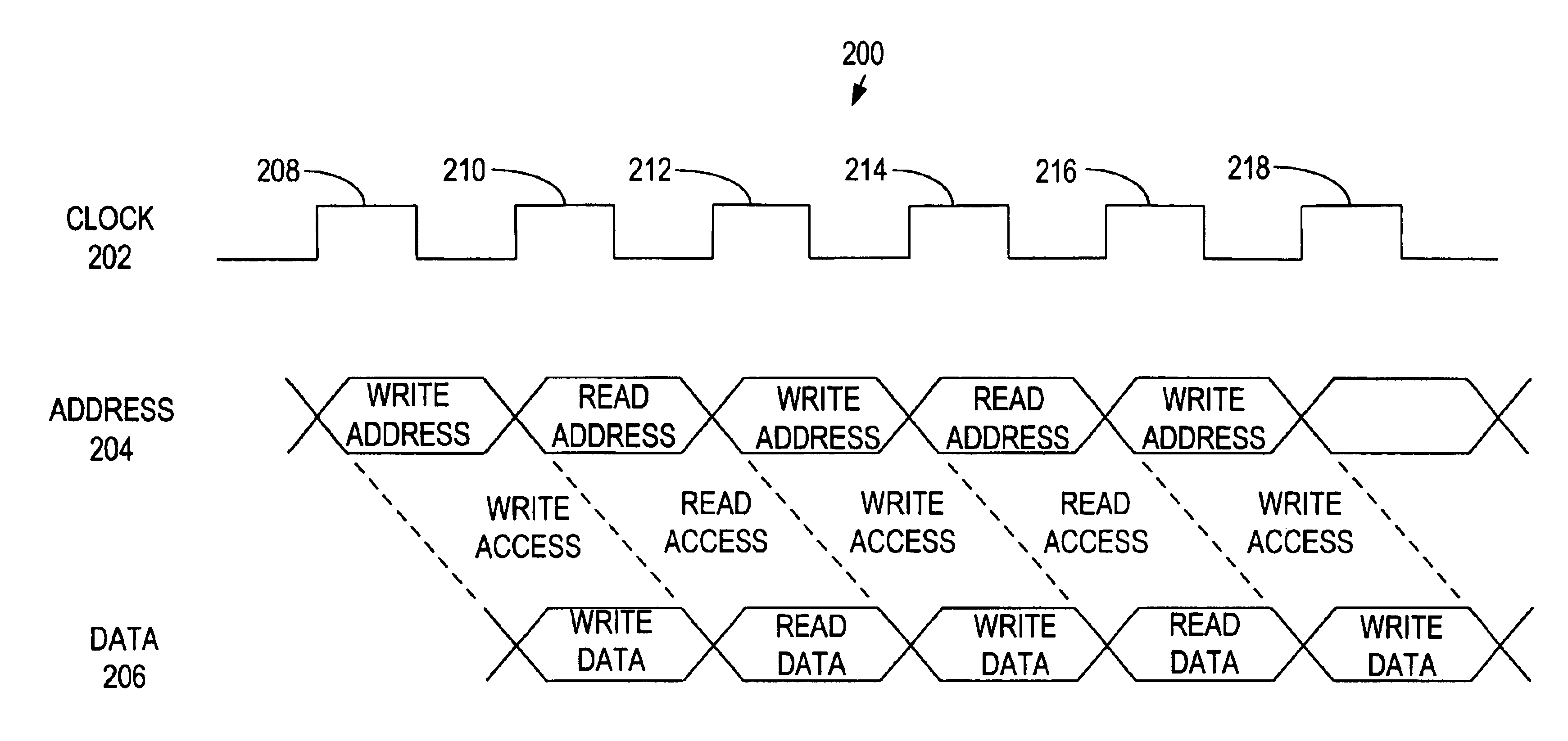
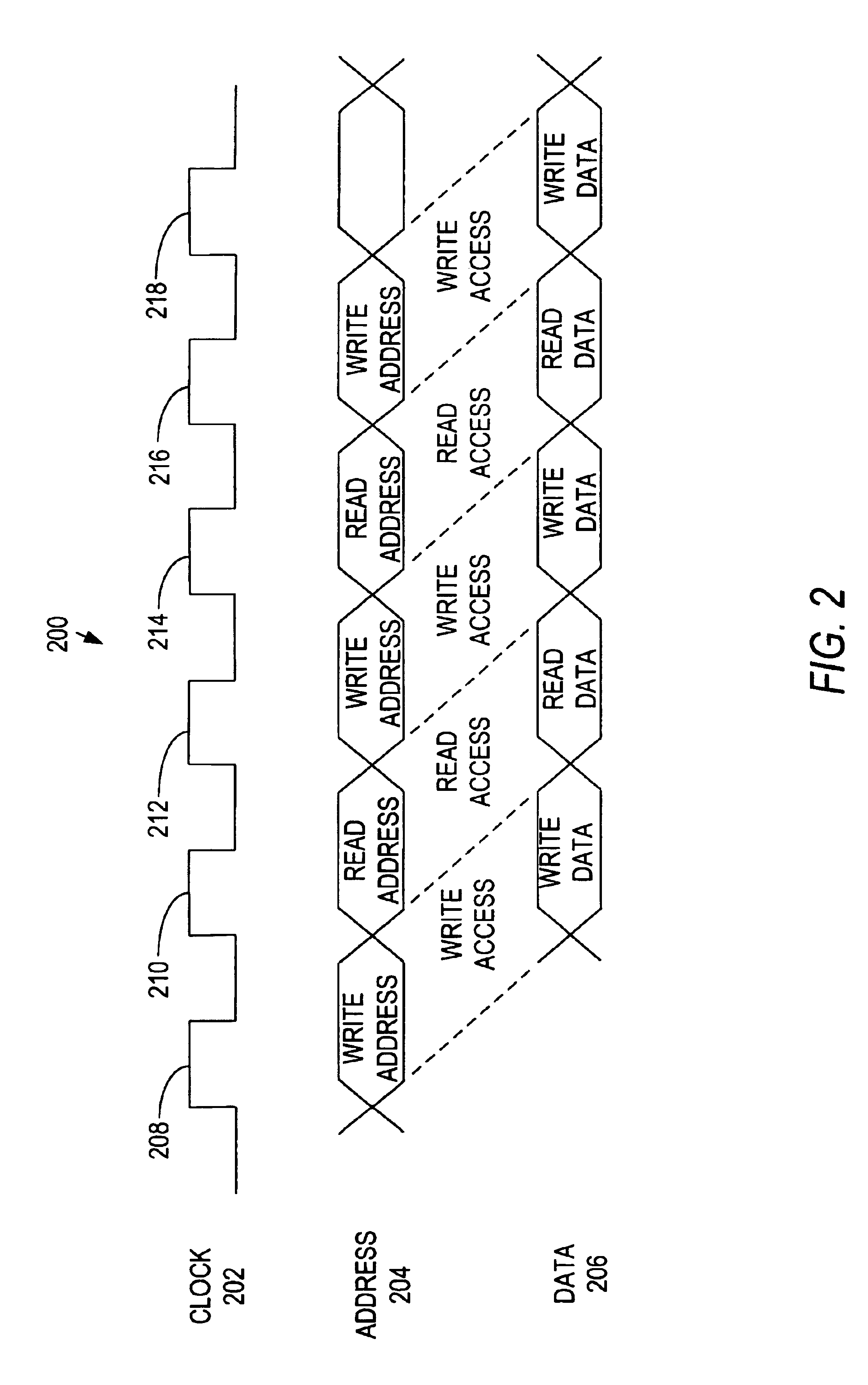
[0006]It is an object of this invention to reduce read-write access delay and write-read access delay in multi-bank memory devices.
[0007]In accordance with the invention, computer circuits that interface with memory devices are provided that have reduced memory access delays. These reduced delays are accomplished by increasing the relative timing between addresses and data for write accesses. This increased relative timing is similar in magnitude to the delay between addresses and data for read accesses. With this adjustment to the relative timing between write addresses and data, read accesses and write accesses can be performed successively with reduced idle time between them.

Problems solved by technology

Advantageously, memory devices are not modified to accommodate the adjusted relative timing with respect to the storage circuits that form the memory storage areas or memory cells of the memory devices.

Method used


Image

  • Multi-bank memory accesses using posted writes
  • Multi-bank memory accesses using posted writes
  • Multi-bank memory accesses using posted writes

Examples


Embodiment Construction

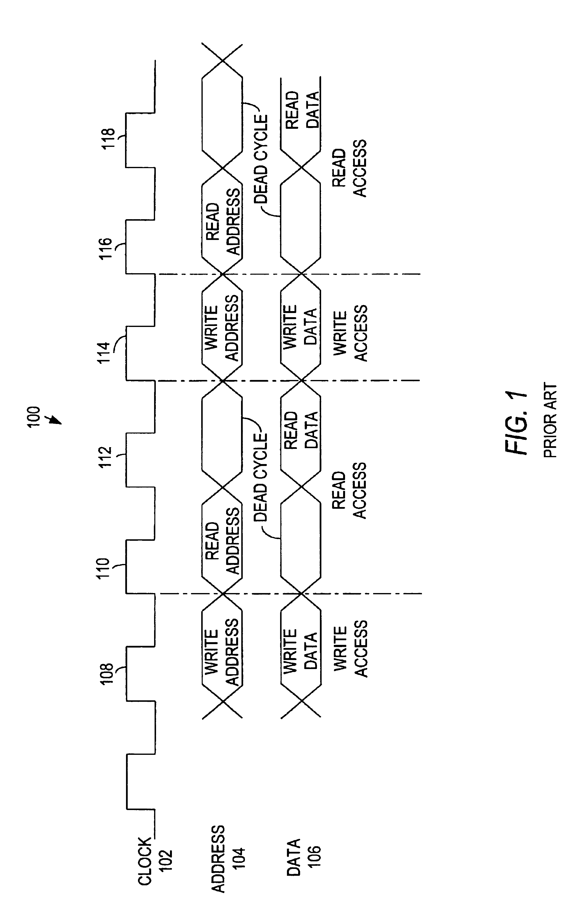
[0016]Memory devices and computer circuits that interface with each other are typically constructed such that addresses and data for write accesses are coincident with each other. For example, with a memory device that has separate address and data busses, computer circuits are typically configured to present addresses and data for a write access during the same clock cycle, or at the same clock edge. Alternatively, data is presented at some other time convenient for the memory device (e.g., data is presented while the memory device is decoding the column address and is inserted into the memory array at a convenient point during the decoding process). Within the memory device itself, addresses and data for write accesses typically retain the same relative timing (i.e., the addresses and data for a write access are present during the same clock cycle or clock edge).

[0017]However, addresses and data for read accesses to memory devices are not coincident during the same clock cycle or ...


PUM


Abstract

Systems and methods for reducing delays between successive write and read accesses in multi-bank memory devices are provided. Computer circuits modify the relative timing between addresses and data of write accesses, reducing delays between successive write and read accesses. Memory devices that interface with these computer circuits use posted write accesses to effectively return the modified relative timing to its original timing before processing the write access.

Description

BACKGROUND OF THE INVENTION[0001]This invention relates to read and write memory accesses in multi-bank memory devices. In particular, this invention relates to reducing the number of clock cycles incurred when accessing multi-bank memory devices.[0002]Computers and other electronic systems usually include memory subsystems. Typical memory subsystems include a memory controller that controls communications between the CPU and various memory devices. Memory devices, such as, for example, DRAMs (dynamic random access memories), are widely used in computer circuits because of their large storage capacity and relatively low power requirements. A DRAM can contain several internal banks of memory cells, which are organized into rows and columns. Typically, a non-banked memory device is one in which the memory device has one memory array with one set of row-column decoding circuitry and one set of data sensing circuitry, while a multi-banked memory device has at least two separate memory a...

Claims


Application Information

Patent Timeline
Patent Type & Authority Patents(United States)
IPC IPC(8): G11C7/10G11C11/4076G11C11/407
CPCG06F12/0207G06F12/0607G11C7/1039G11C7/1072G11C11/4076G11C2207/2218G11C2207/229
Inventor PAWLOWSKI, J. THOMAS
Owner ROUND ROCK RES LLC
Learn More