

Multi-bank memory accesses using posted writes
a multi-bank memory and write-in technology, applied in the field of read and write memory accesses in multi-bank memory, can solve the problem that the memory device cannot be modified to accommodate the adjusted relative timing, and achieve the effect of reducing the read-write access delay and the write-read access delay
- Summary
- Abstract
- Description
- Claims
- Application Information
AI Technical Summary
Benefits of technology
Problems solved by technology
Method used
Image

Examples
Embodiment Construction
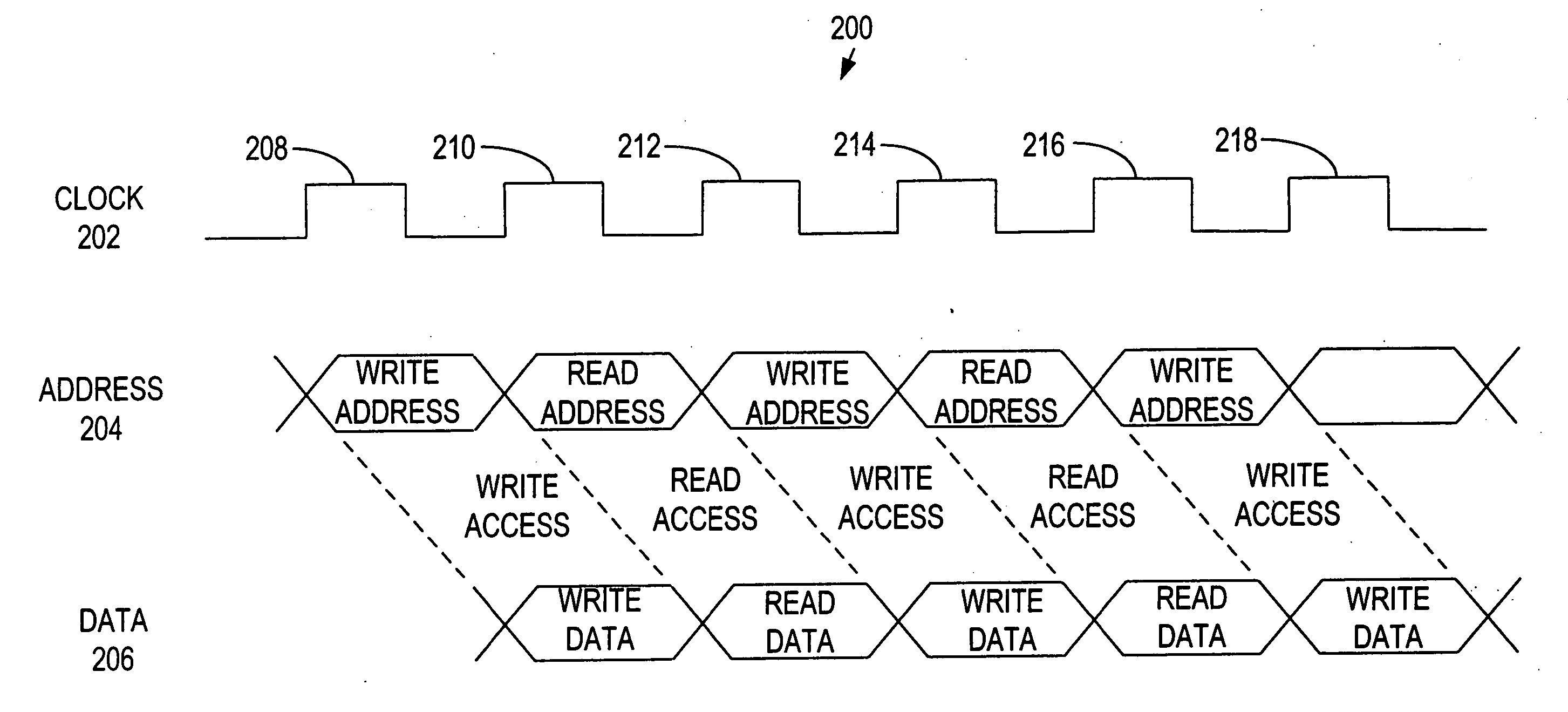
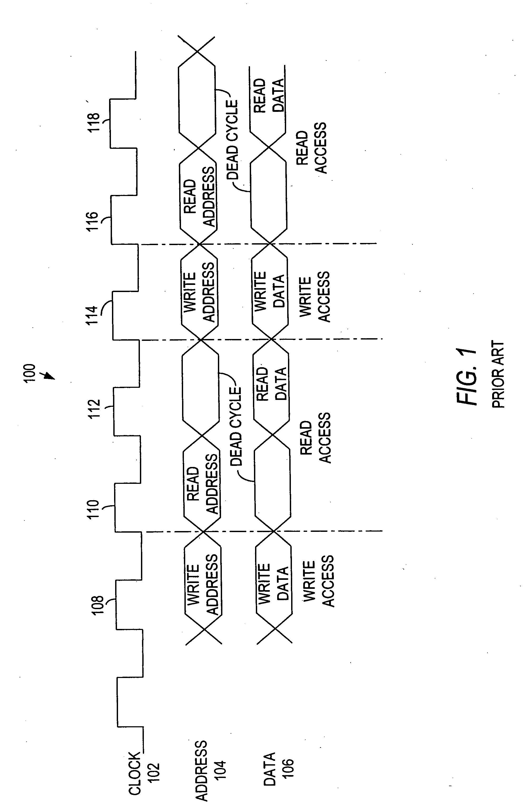
[0016] Memory devices and computer circuits that interface with each other are typically constructed such that addresses and data for write accesses are coincident with each other. For example, with a memory device that has separate address and data busses, computer circuits are typically configured to present addresses and data for a write access during the same clock cycle, or at the same clock edge. Alternatively, data is presented at some other time convenient for the memory device (e.g., data is presented while the memory device is decoding the column address and is inserted into the memory array at a convenient point during the decoding process). Within the memory device itself, addresses and data for write accesses typically retain the same relative timing (i.e., the addresses and data for a write access are present during the same clock cycle or clock edge).
[0017] However, addresses and data for read accesses to memory devices are not coincident during the same clock cycle ...
PUM
 Abstract
Description
Claims
Application Information