Data processor and graphic data processing device

a data processor and graphic data technology, applied in the field of graphic data processors, can solve the problems of unnecessarily long wait time until the cpu obtains the right of the pixel bus, the data transfer latency deteriorates, and the cpu may deteriorate the data processing speed, so as to increase the speed of the data transfer with the central processing unit, increase the wait time, and increase the effect of the speed of the graphic data processing

Active Publication Date: 2005-02-10
RENESAS ELECTRONICS CORP
View PDF12 Cites 24 Cited by
  • Summary
  • Abstract
  • Description
  • Claims
  • Application Information

AI Technical Summary

Benefits of technology

[0014] With the means, by directly connecting the central processing unit to the first bus, it becomes unnecessary to interpose a bus controller and the like between them. The speed of a data transfer with the central processing unit can be increased by the amount. In the case where the central processing unit has a super scalar structure of issuing a plurality of commands in one cycle, the command processing capability about twice as high as the operating frequency can be obtained. When an object to be accessed, which is necessary for executing the command, is an external memory coupled via the first bus, the access speed is controlled to the access efficiency on the first bus. At this time, by connecting only the first circuit modules selected from the viewpoint of the degree of importance of realizing higher speed of the graphic data processing to the first bus, increase in wait time caused by access competition on the first bus is suppressed and it can contribute to improve the data processing speed of the central processing unit.
[0015] Since only the CPU and the DMA serve as bus masters on the first bus, the case where the CPU waits for a transfer request on the first bus hardly occurs. The first circuit modules such as the graphic processing module are subjected to arbitration in advance by a bus arbitration logic for the second bus. After the graphic processing circuit module truly requested to have real-time response is selected, bus right arbitration on the first bus between the CPU and the three-dimensional graphic module is executed. The graphic processing circuit module is requested to have real-time response, that is, high throughput performance but is not requested to achieve access latency reduced as much as that of the CPU. The bus arbitration logic in the memory interface circuit executes bus right arbitration among three requests of an access request from the three-dimensional graphic module, an access request from the circuit module connected to the first subs, and an access request using the second bus. Therefore, only the CPU and modules truly requiring high-speed transfer can be connected to the first bus, so that the higher speed of the bus can be easily achieved. Since the first circuit modules such as the graphic processing module is arbitrated by the bus arbitration logic on the second bus, real-time response performance of the graphic processing circuit modules is not substantially disturbed.
[0016] Since the first and second buses are separated from each other, collision between an access to a peripheral circuit module of the CPU and memory data transfer of the graphic processing circuit module hardly occurs. Therefore, without deteriorating the latency of the CPU access, data transfer with the peripheral circuit module can be performed.
[0017] By connecting the three-dimensional graphic processor to the first bus, necessity of performing a transfer of operands such as commands and a large amount of vertex data with the three-dimensional graphic processor in a three-dimensional graphic process can be satisfied. Further, in the three-dimensional graphic process, a large amount of graphics data has to be frequently sent / received to / from the memory at the time of hidden-surface removal and texture mapping in the step of processing vertex data. As compared with the other graphic processing circuit modules, not only high throughput but also suppressed access latency is needed. With the configuration in which the three-dimensional graphic processor is directly connected to the memory interface circuit via a dedicated bus, the requirements can be satisfied.

Problems solved by technology

First, since the CPU is provided on the outside of the graphic data processor and accesses the graphic data processor and the data memory via the CPU interface, data transfer latency deteriorates.
Second, it is feared that transfer between a peripheral module and the data memory or transfer between the graphic module and the data memory and transfer between the CPU and the data memory compete with each other on the pixel bus.
Such competition may deteriorate data processing speed of the CPU.
In this case, wait time until the CPU obtains the right of the pixel bus may become unnecessarily long.
Third, since there is no dedicated DMAC on the pixel bus, data from the CPU or a device on the CPU bus to the data memory has to be transferred by sequential transfer under control of the CPU or by using resources of a DMA channel of the CPU.
Consequently, it is expected that the CPU is overloaded.
The inventors have found that the thick line drawing has a problem such that, when a method of sequentially filling pixels from the start point to the end point with color is employed, if the drawing directions are different from each other, even if the number of lines in which pixels from the start and end points are filled with color is the same, the width of a thick line varies.

Method used


Image

  • Data processor and graphic data processing device
  • Data processor and graphic data processing device
  • Data processor and graphic data processing device

Examples


Embodiment Construction

[0052] Graphic Data Processor

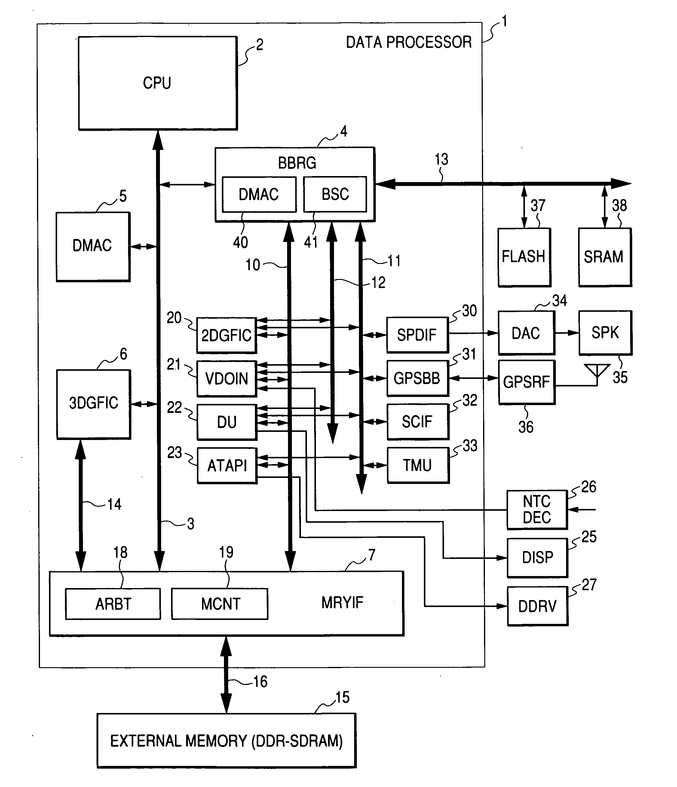
[0053]FIG. 1 illustrates a navigation system using a graphic data processor according to an embodiment of the invention. A graphic data processor 1 shown in FIG. 1 is, although not limited, formed on a single semiconductor substrate (semiconductor chip) made of single crystal silicon or the like by a complementary MOS (CMOS) integrated circuit manufacturing technique, or the graphic data processor is included in one package comprising a plurality of semiconductor chips including graphic data processor and memory module or the like.

[0054] The graphic data processor 1 has therein a CPU (Central Processing Unit) 2. To a first bus 3 to which the CPU 2 is connected, a bus bridge circuit (BBRG) 4, a direct memory access controller (DMAC) 5, a 3D graphics module (3DGFIC) 6 as a three-dimensional graphics data processing module for performing a three-dimensional graphic data processing such as a process of drawing a three-dimensional image, and a memory interf...


PUM


Abstract

An object of the present invention is to improve efficiency of transfer of control information, graphic data, and the like for drawing and display control in a graphic data processor. A graphic data processor includes: a CPU; a first bus coupled to the CPU; a DMAC for controlling a data transfer using the first bus; a bus bridge circuit for transmitting/receiving data to/from the first bus; a three-dimensional graphics module for receiving a command from the CPU via the first bus and performing a three-dimensional graphic process; a second bus coupled to the bus bridge circuit and a plurality of first circuit modules; a third bus coupled to the bus bridge circuit and second circuit modules; and a memory interface circuit coupled to the first and second buses and the three-dimensional graphic module and connectable to an external memory, wherein the bus bridge circuit can control a direct memory access transfer between an external circuit and the second bus.

Description

CROSS-REFERENCE TO RELATED APPLICATION [0001] The present application claims priority from Japanese patent application JP 2003-206466 filed on Aug. 7, 2003, the content of which is hereby incorporated by reference into this application. BACKGROUND OF THE INVENTION [0002] The present invention relates to a graphic data processor formed on a semiconductor chip and, more particularly, to a technique effective when applied to fields requiring graphic data processing of, for example, a car information system, a set-top box, a digital TV, a mobile communication system, a digital sound terminal, a media terminal, a portable terminal, and the like. [0003] Japanese Unexamined Patent Publication No. 2003-208631 (FIG. 32) describes a graphic processor for performing a three-dimensional graphics process. Japanese Unexamined Patent Publication No. Hei 6(1994)-28486 (FIG. 1) discloses a graphic processor having a thick line drawing function. [0004] The inventors herein have examined optimization ...

Claims


Application Information

Patent Timeline
Patent Type & Authority Applications(United States)
IPC IPC(8): G06F13/28G06F15/78G06T1/20G06T11/20G06T11/40G06T15/00
CPCG06T11/203G06T1/20
Inventor HARA, HIROTAKAHAMASAKI, HIROYUKISAEKI, MITSUHIROHIRADE, KAZUHIROTAKANO, MAKOTO
Owner RENESAS ELECTRONICS CORP
Why Eureka
Try Eureka