Ball grid array package with an electromagnetic shield connected directly to a printed circuit board

a technology of electromagnetic shield and printed circuit board, which is applied in the direction of cross-talk/noise/interference reduction, electrical apparatus construction details, and electrical apparatus casings/cabinets/drawers, etc., and can solve problems such as material fatigue or damage to solder bumps, shortening the service life of solder bumps

Inactive Publication Date: 2005-09-20
BENQ CORP
View PDF12 Cites 84 Cited by
  • Summary
  • Abstract
  • Description
  • Claims
  • Application Information

AI Technical Summary

Problems solved by technology

The conventional BGA package is disadvantageous in that impacts or stress applied to the electromagnetic shield 54 is transmitted to the printed circuit board 53 t

Method used


Image

  • Ball grid array package with an electromagnetic shield connected directly to a printed circuit board
  • Ball grid array package with an electromagnetic shield connected directly to a printed circuit board
  • Ball grid array package with an electromagnetic shield connected directly to a printed circuit board

Examples


Embodiment Construction

[0023]For the sake of brevity, like elements are denoted by the same reference numerals throughout the disclosure.

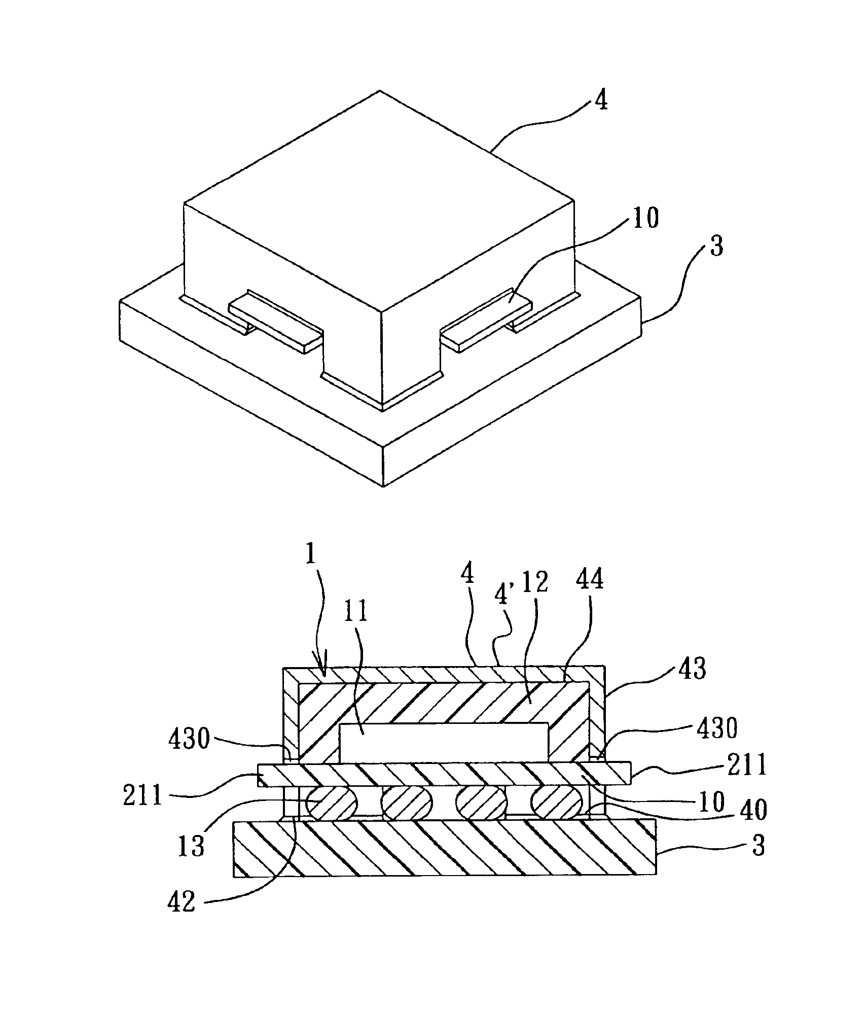
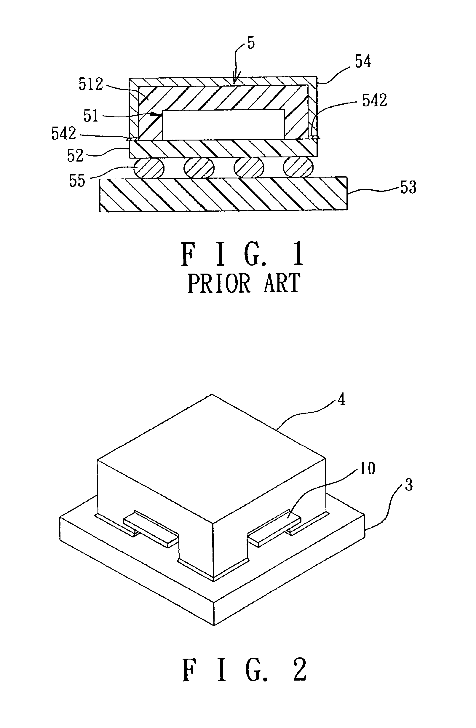
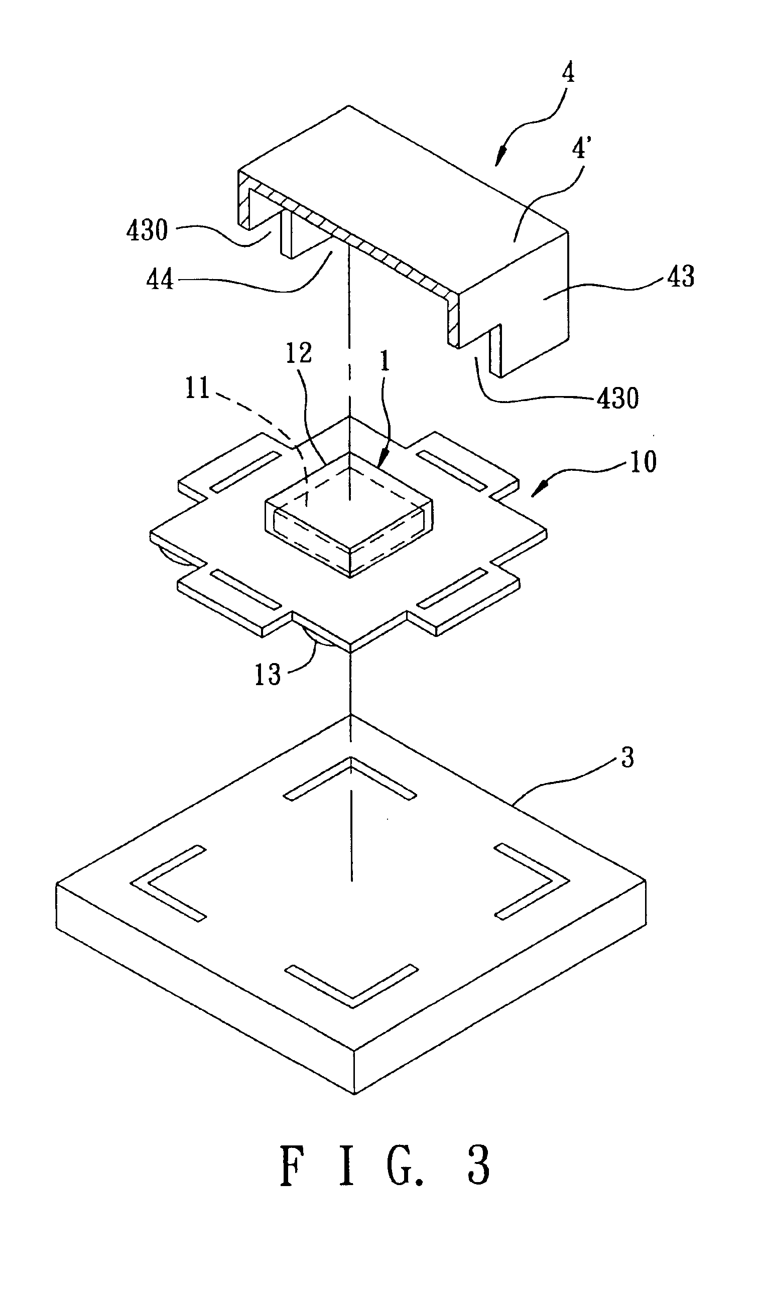
[0024]FIGS. 2 to 4 illustrate the first preferred embodiment of an electronic device according to the present invention. The electronic device includes a ball grid array (BGA) package connected electrically to a printed circuit board 3.

[0025]The BGA package includes: a chip 1 having a substrate 10 with opposite top and bottom surfaces, and a semiconductor die 11 mounted on the top surface of the substrate 10 and enclosed by an encapsulant 12; a plurality of solder bumps 13 projecting outwardly from the bottom surface of the substrate 10 and connected directly and electrically to the printed circuit board 3; and an electromagnetic shield 4 including a housing 4′ that defines an inner space 44 which receives the chip 1 and the solder bumps 13 therein, and a bottom opening 40 for access into the inner space 44. The solder bumps 13 project outwardly of the inner space 44 thr...


PUM


Abstract

A ball grid array package includes a chip having a substrate with a bottom surface, a plurality of solder bumps projecting outwardly from the bottom surface of the substrate, and an electromagnetic shield including a housing that defines an inner space which receives the chip and the solder bumps therein, and a bottom opening for access into the inner space. The solder bumps project outwardly of the inner space through the bottom opening in the housing.

Description

CROSS-REFERENCE TO RELATED APPLICATION[0001]This application claims priority of Taiwanese application No. 092200989, filed on Jan. 20, 2003.BACKGROUND OF THE INVENTION[0002]1. Field of the Invention[0003]This invention relates to a ball grid array package, more particularly to a ball grid array package with an electromagnetic shield connected directly to a printed circuit board.[0004]2. Description of the Related Art[0005]FIG. 1 illustrates a conventional ball grid array (BGA) package that includes a chip 5 having a substrate 52 and a semiconductor die 51 mounted on the substrate 52 and enclosed by an encapsulant 512 of an insulating material. An electromagnetic shield 54 is provided to enclose the encapsulant 512 so as to minimize electromagnetic interference on the die 51. The electromagnetic shield 54 includes a housing that has a bottom end 542 connected to the substrate 52 by welding. The BGA package is connected electrically to a printed circuit board 53 through a plurality of...

Claims


Application Information

Patent Timeline
IPC IPC(8): H01L23/31H01L23/28H01L23/552H05K3/34H05K1/02
CPCH01L23/3128H01L23/552H01L2924/15311H01L2924/16152H01L2924/3025H05K1/0218H05K3/3436H01L2924/0002H01L2924/00
Inventor HSIEH, CHIA-MING
Owner BENQ CORP
Why Eureka
Try Eureka