Tool suite for the rapid development of advanced standard cell libraries employing the connection properties of nets to identify potential pin placements

a technology of connecting properties and cell libraries, applied in the field of automatic design techniques of electronic circuits, can solve the problems of complex modern chips, possible flaws in the physical design of the chip, and the process of creating layout for individual cells requires substantial manual intervention for each cell, so as to increase the speed, automation and accuracy of creating physical designs.

Inactive Publication Date: 2005-09-20
FRANTORF INVESTMENTS
View PDF14 Cites 30 Cited by
  • Summary
  • Abstract
  • Description
  • Claims
  • Application Information

AI Technical Summary

Benefits of technology

[0013]The above described problems and needs associated with automated chip design are addressed with a library tool suite according to embodiments of the present invention. The library tool suite supplements conventional design tools to increase the speed, automation and accuracy of creating physical designs for a library of cells to be used in chip designs. The tool suite may include a post operations tool, an audit tool, a custom interface, a setup file and a place and route model preparation utility which interact with the conventional tools and design data to automate and ensure integrity of the physical design process.
[0014]The tool suite facilitates automatically generating libraries corresponding to an overall cell plan, generating attributes defining a strength of connection between possible pin placements within a cell to facilitate routing inter-cell nets through the cell, and auditing cells for errors prior to inclusion in a manufacturing library.

Problems solved by technology

This is challenging because modern chips are very complex, including millions of transistors and often a mile or more of wire interconnecting the transistors.
For example, conventionally, the process of creating layout for individual cells requires substantial manual intervention for each cell.
Thus, conventional processes leave the possibility for flaws in the physical design of the chip.

Method used


Image

  • Tool suite for the rapid development of advanced standard cell libraries employing the connection properties of nets to identify potential pin placements
  • Tool suite for the rapid development of advanced standard cell libraries employing the connection properties of nets to identify potential pin placements
  • Tool suite for the rapid development of advanced standard cell libraries employing the connection properties of nets to identify potential pin placements

Examples


Embodiment Construction

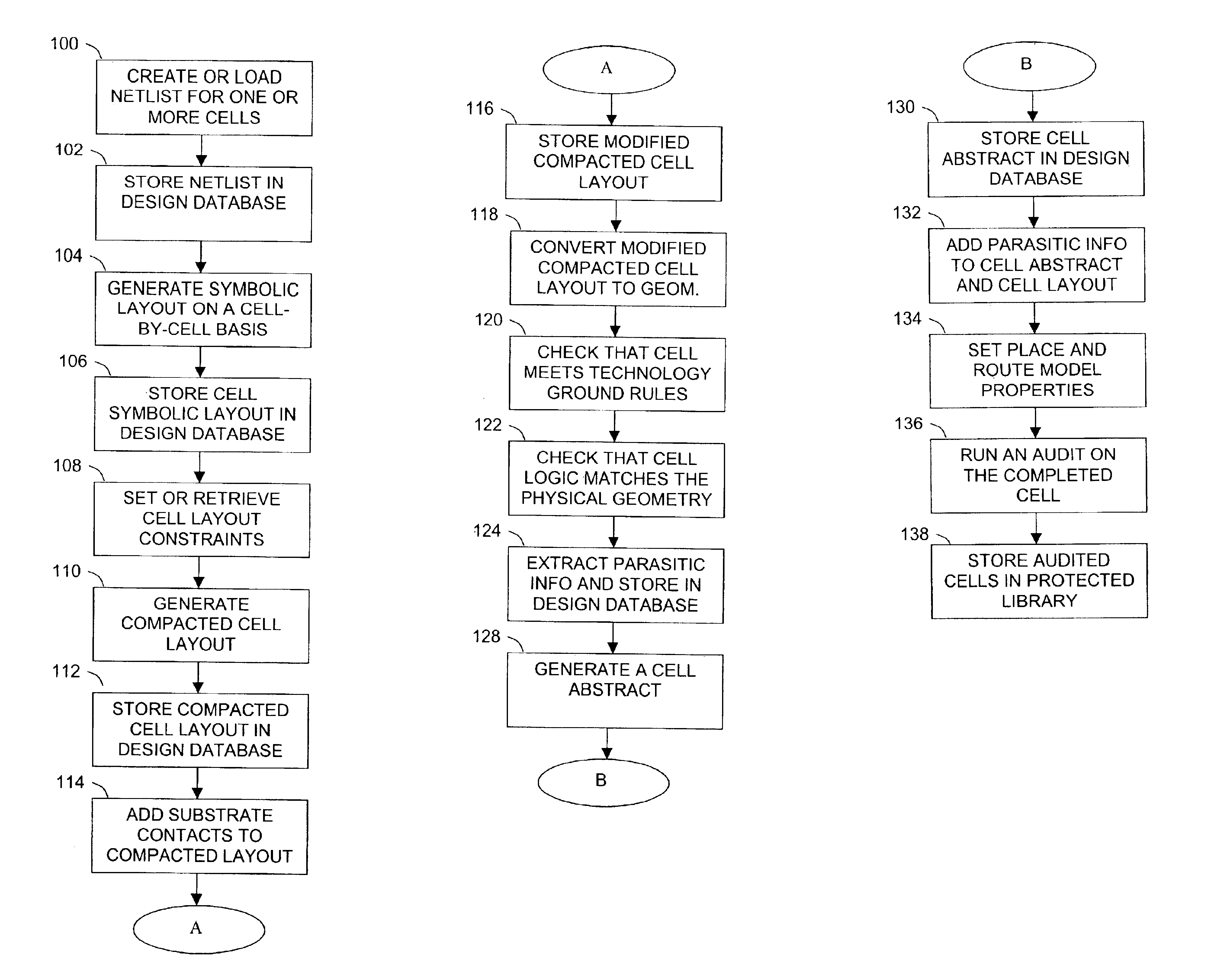
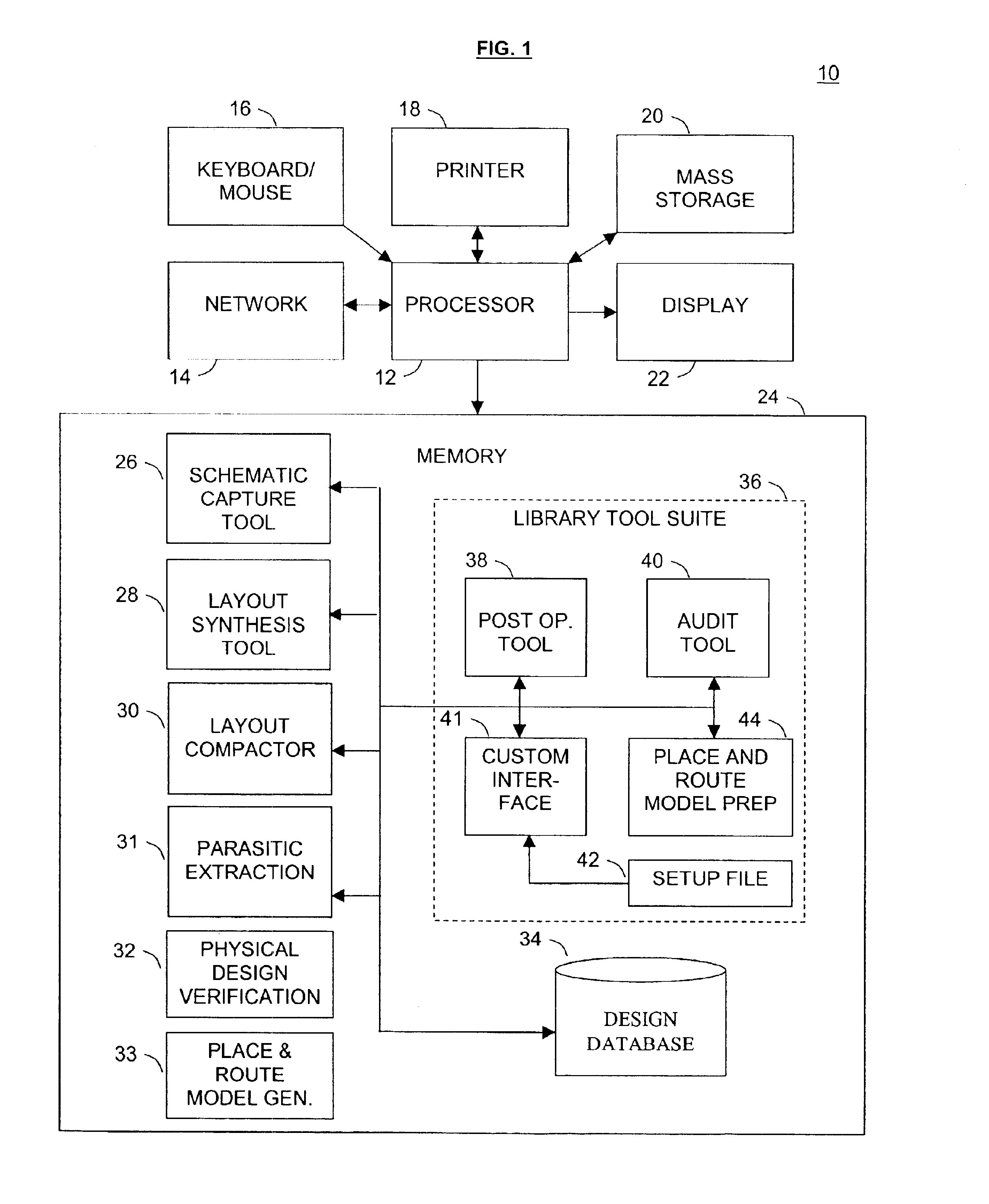
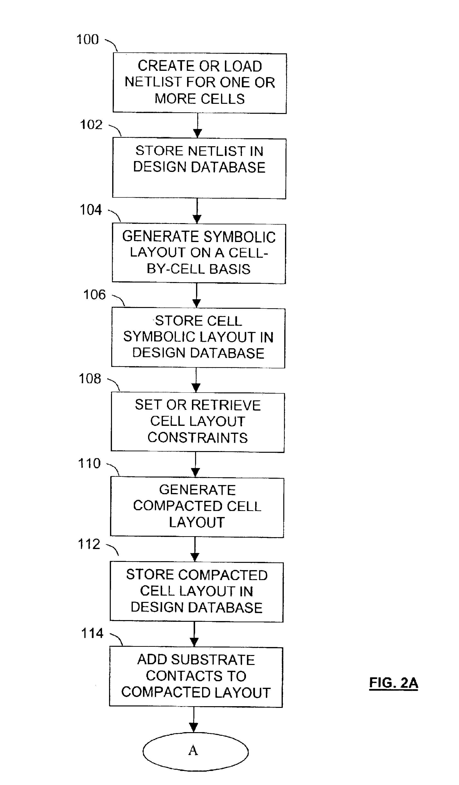
[0029]FIG. 1 depicts a system 10 for performing automated design of an electronic circuit, such as an integrated circuit chip. The system 10 includes a processor 12, coupled to a network 14, input devices 16, a printer 18, a mass storage device 20, a display 22 and a memory 24.

[0030]The memory 24 may include random access memory (RAM) and / or read only memory (ROM) and other storage devices for storing information on and reading information from a computer useable medium. The other storage devices may illustratively include hard and floppy disk drives, tape drive and compact disk (CD) ROM and video disk drives. The memory 24 stores program instructions for commanding the processor 12 of the system 10 to perform design functions. For example, the memory 24 includes program instructions for a schematic capture tool 26, a layout synthesis tool 28, a layout compactor tool 30, a parasitic extraction tool 31, a physical design verification tool 32, a place and route model generation tool 3...


PUM


Abstract

A library tool suite supplements conventional design tools to increase the speed, automation and accuracy of creating physical designs for a library of cells to be used in chip designs. The tool suite may include a post operations tool, an audit tool, a custom interface, a setup file and a place and route model preparation utility which interact with the conventional tools and design data to automate and ensure integrity of the physical design process. The tool suite facilitates automatically generating libraries corresponding to an overall cell plan, generating attributes defining strength of connection between possible pin placements within a cell to facilitate routing inter-cell nets through a cell, and auditing cells for errors prior to inclusion in a manufacturing library.

Description

CROSS-REFERENCE TO RELATED APPLICATION[0001]This application is a divisional of application Ser. No. 09 / 597,229, filed Jun. 20, 2000 now U.S. Pat. No. 6,539,533.FIELD OF THE INVENTION[0002]The present invention relates generally to the field of automated design techniques for electronic circuits and, more particularly, to methods and systems for efficiently generating and checking physical layouts corresponding to libraries of electronic circuit cells.BACKGROUND OF THE INVENTION[0003]Semiconductor manufacturing technology is constantly changing and advancing to realize smaller feature sizes in manufacturing, thus permitting the manufacture of faster, more dense and power efficient electronic circuits. Semiconductor chips, such as application specific integrated circuit chips (“ASICs”) and custom logic chips, such as microprocessors and memories, are designed in this environment of change, often on short design schedules.[0004]In order to utilize the latest changes and advances in se...

Claims


Application Information

Patent Timeline
Patent Type & Authority Patents(United States)
IPC IPC(8): G06F17/50H01L27/118
CPCG06F17/5068H01L27/118G06F30/39
Inventor BROWN, III, ARNETT J.STALKER, ROBERT J.LAKHANI, RAJEN NARANNEIDERER, ERIC WAYNEBAYLES, DEVIN
Owner FRANTORF INVESTMENTS
Why Eureka
Try Eureka