Semiconductor manufacturing line availability evaluating system and design system

a technology of availability evaluation and manufacturing line, applied in the direction of electric programme control, instruments, computing, etc., can solve the problems of not being provided a technique capable of simply evaluating such an effect, and the effect of greatly affecting the availability of the fabrication line is not easy to replace the polishing pad

Inactive Publication Date: 2006-01-03
KK TOSHIBA
View PDF3 Cites 5 Cited by
  • Summary
  • Abstract
  • Description
  • Claims
  • Application Information

AI Technical Summary

Problems solved by technology

If such a one-tool unit stops, the fabrication availability of the line is greatly affected.
Thus, no lot flow stoppage occurs, but an effect on the fabrication availability of the line cannot be ignored.
Conventionally, there has not been provided a technique capable of simply evaluating such an effect.
A total number of tools per line increases, thus having caused an increase of tool investment, an increase of running cost, and an increase of clean room space.
From among them, it has been extremely difficult to evaluate an availability of a line in consideration of an effect on the line fabrication productivity when one or more tools stop(s).
In addition, one-tool units are mainly provided in a small scale semiconductor manufacturing line, and thus, the lowering of the line availability caused by a failure of such a one-tool unit has been a large problem.

Method used


Image

  • Semiconductor manufacturing line availability evaluating system and design system
  • Semiconductor manufacturing line availability evaluating system and design system
  • Semiconductor manufacturing line availability evaluating system and design system

Examples


first embodiment

(First Embodiment)

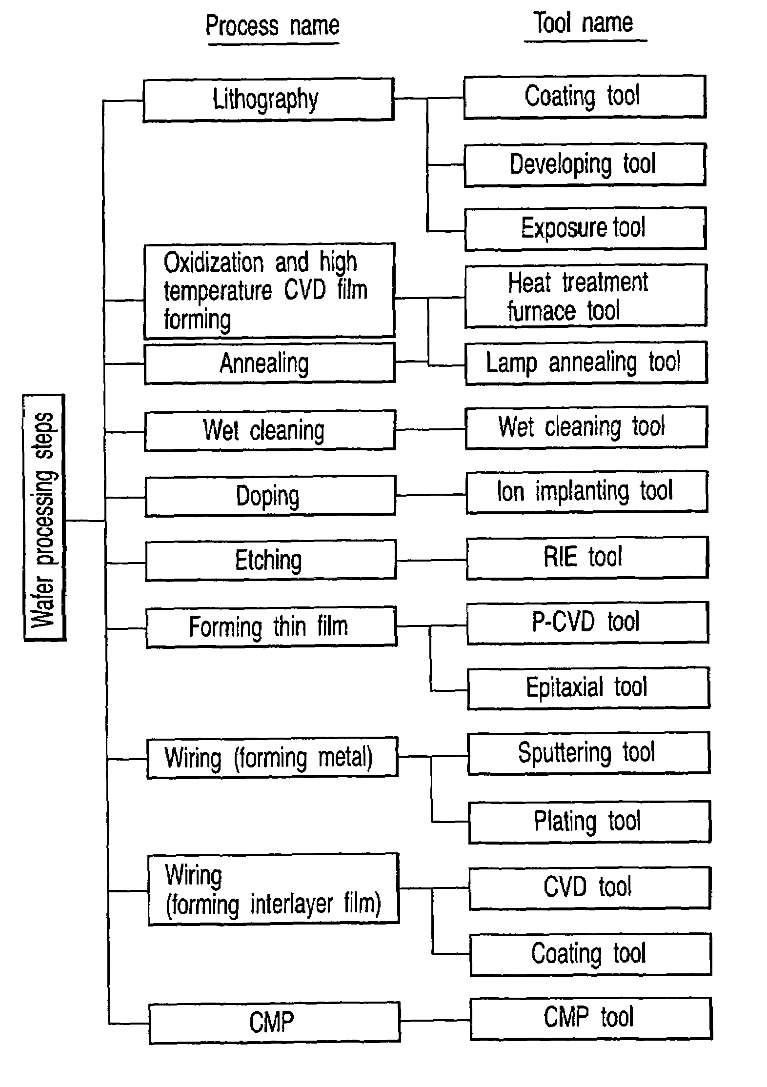
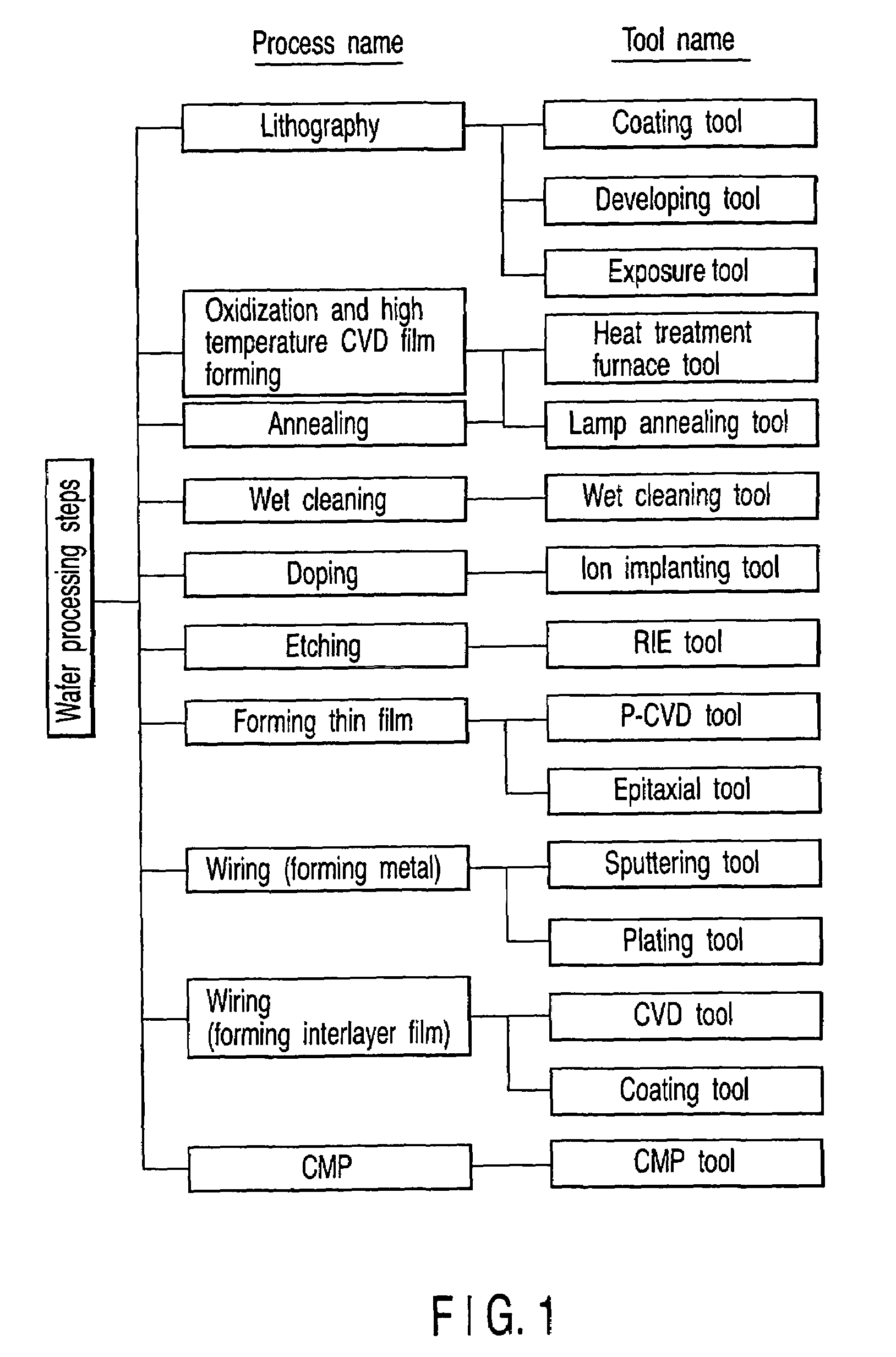
[0050]For example, in wafer processing included in a semiconductor manufacturing line, the types of process are roughly divided into 10 processes as shown in FIG. 1, and an illustrated dedicated process tool is provided in accordance with each of the steps. That is, a coating tool, a developing tool, an exposure tool and the like are provided for a lithography process. A heat treatment furnace tool and a lamp annealing tool are provided for oxidization and high temperature CVD film and annealing steps, respectively. A wet cleaning tool is provided for a wet cleaning process. An ion implantation tool is provided for a doping process. An RIE tool is provided for an etching process. A P-CVD tool, an epitaxial tool and the like are provided for a thin film forming process. A sputtering tool, a plating tool and the like are provided for a wiring (metal forming) process. A CVD tool, a coating tool and the like are provided for a wiring (interlayer film forming) process. ...

second embodiment

(Second Embodiment)

[0093]In the first embodiment, the line availability has been obtained by checking all combinations of operation and stoppage of tools each configuring a line; incorporating the probabilities of operation and stoppage into the combinations; obtaining the incidence probability of each of the combinations; multiplying the production capabilities of that combination; and obtaining a sum of all the combinations. Although this method can obtain the line availability precisely, there is a problem that a large amount of time is required if a large number of cases exist in the case of obtaining all the combinations.

[0094]For example, several hundreds of tools are equipped in a line having a fabrication capability of 1000 Lots per month, and 10 or more tools are required for the same step. In this case, the number of combinations is deemed to be the second power of the number of tools. For example, if 300 tools exist in a line, combinations of 2300 can be assumed. It is su...

third embodiment

(Third Embodiment)

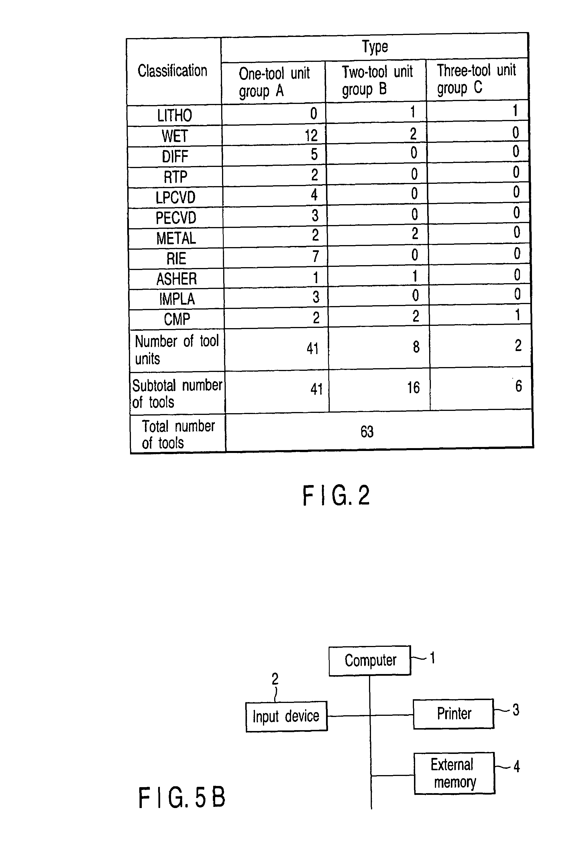
[0108]The first embodiment has described as an example of reducing the number of one-tool units by sharing a processing tool among several steps and improving a line availability. A method of reducing the number of one-tool units includes introducing at least one tool of the same unit type to configure a two-tool unit and increase the line availability. In this manner, even if one tool in the two-tool unit stops, the other tool can continue processing step. In this method, there is a disadvantage that fabrication cost increases, although it is simple because the completely same tool is merely purchased. However, increasing the line availability is worthy because, the fabrication output increases concurrently and the term of work or the TAT is also reduced.

[0109]FIG. 31 shows a result of calculating the line availability when the same type of tool or tools have been redundantly introduced with respect to a line in which 21 one-tool units and 6 two-tool units exist. ...


PUM


Abstract

An availability evaluation system of a semiconductor manufacturing line, comprising a unit configured to calculate an incidence probability Xi (i=1 to k) in combination by applying a tool operation probability and a tool stoppage probability to all combinations “k” in which at least a line fabrication availability is not zero, of the combinations of operation and stoppage of tools, and by obtaining a product of the probabilities of all the tools, and a unit configured to, when a product between the incidence probability Xi of a combination and a fabrication availability Yi of the combination is defined as a probability converted fabrication availability with respect to each of the combinations, calculate an availability value of Q=Σ(i=1 to k)X1×Y1 / F obtained by dividing a sum of probability converted fabrication availabilities of the combinations by a fabrication availability F at a 100% availability.

Description

CROSS-REFERENCE TO RELATED APPLICATIONS[0001]This application is based upon and claims the benefit of priority from the prior Japanese Patent Application No. 2003-336248, filed on Sep. 26, 2003, the entire contents of which are incorporated herein by reference.BACKGROUND OF THE INVENTION[0002]1. Field of the Invention[0003]The present invention relates to an availability evaluating system for evaluating an availability of a semiconductor manufacturing line which includes a plurality of semiconductor manufacturing tools and a semiconductor manufacturing line design system for designing a semiconductor manufacturing line with a high availability.[0004]2. Description of the Related Art[0005]In a semiconductor manufacturing line for fabricating a semiconductor device such as an LSI, it is necessary to equip a plurality of semiconductor manufacturing tools for forming a very small transistors, for example, and further, form metal wirings by applying a variety of processing operations ont...

Claims


Application Information

Patent Timeline
Patent Type & Authority Patents(United States)
IPC IPC(8): G06F19/00G05B19/418H01L21/00H01L21/02
CPCH01L21/67276
Inventor MIKATA, YUUICHI
Owner KK TOSHIBA
Why Eureka
Try Eureka