Multi-domain liquid crystal display device having pixel electrodes with electric field inducing windows

a liquid crystal display device and pixel electrode technology, applied in non-linear optics, instruments, optics, etc., can solve the problems of weak electric field distortion needed to divide the pixel region, decrease in brightness, etc., and achieve high response time characteristics, stable arrangement of liquid crystal molecules, and high brightness

Inactive Publication Date: 2006-01-31
LG DISPLAY CO LTD
View PDF40 Cites 16 Cited by
  • Summary
  • Abstract
  • Description
  • Claims
  • Application Information

AI Technical Summary

Benefits of technology

[0014]An object of the present invention is to provide a multi-domain LCD having high response time characteristics and high brightness by stable arrangement of liquid crystal molecules.

Problems solved by technology

If the electrodes do not have an open area or the width of the open area is narrow, the electric field distortion needed to divide the pixel region becomes weak.
At this time, disclination occurs from the area where the liquid crystal directors are parallel with a transmittance axis of the polarizer, which results in a decrease in brightness.

Method used


Image

  • Multi-domain liquid crystal display device having pixel electrodes with electric field inducing windows
  • Multi-domain liquid crystal display device having pixel electrodes with electric field inducing windows
  • Multi-domain liquid crystal display device having pixel electrodes with electric field inducing windows

Examples


Embodiment Construction

[0035]Hereinafter, the multi-domain liquid crystal display device of the present invention is explained in detail by accompanying the drawings.

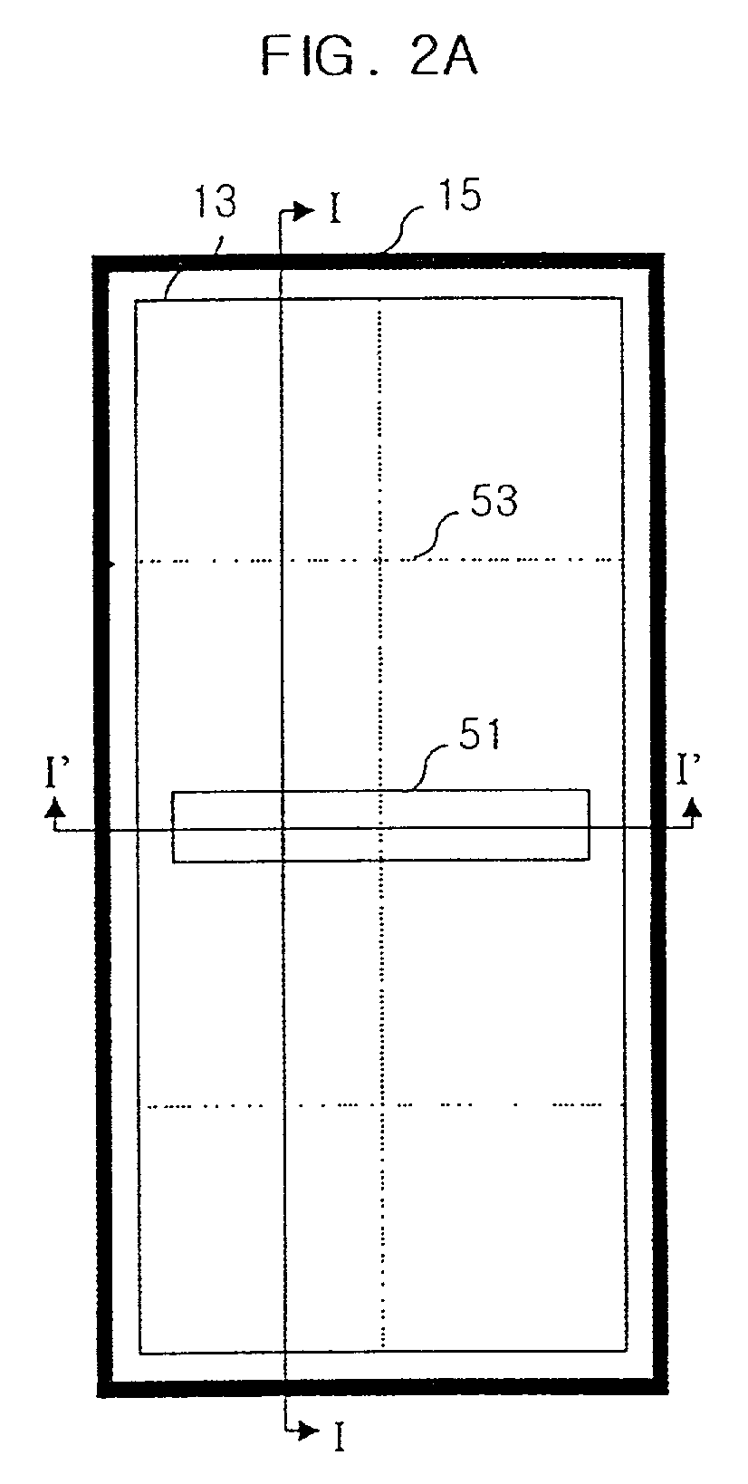
[0036]FIGS. 2A, 2B, 2C, 2D, 2E, and 2F are plan views of the multi-domain liquid crystal display devices according to the embodiments of the present invention, FIGS. 3A, 3B, 3C, 3D, and 3E are sectional views taken along the lines I—I and I′—I′ of FIG. 2A according to the embodiments of the present invention.

[0037]FIGS. 4A, 4B, 4C, 4D, 4E, and 4F are plan views of the multi-domain liquid crystal display devices according to the embodiments of the present invention, FIGS. 5A, 5B, 5C, 5D, and 5E are sectional views taken along the lines II—II and II′—II′ of FIG. 4A according to the embodiments of the present invention.

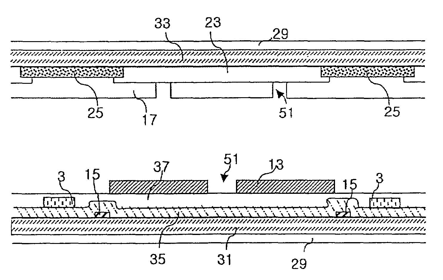
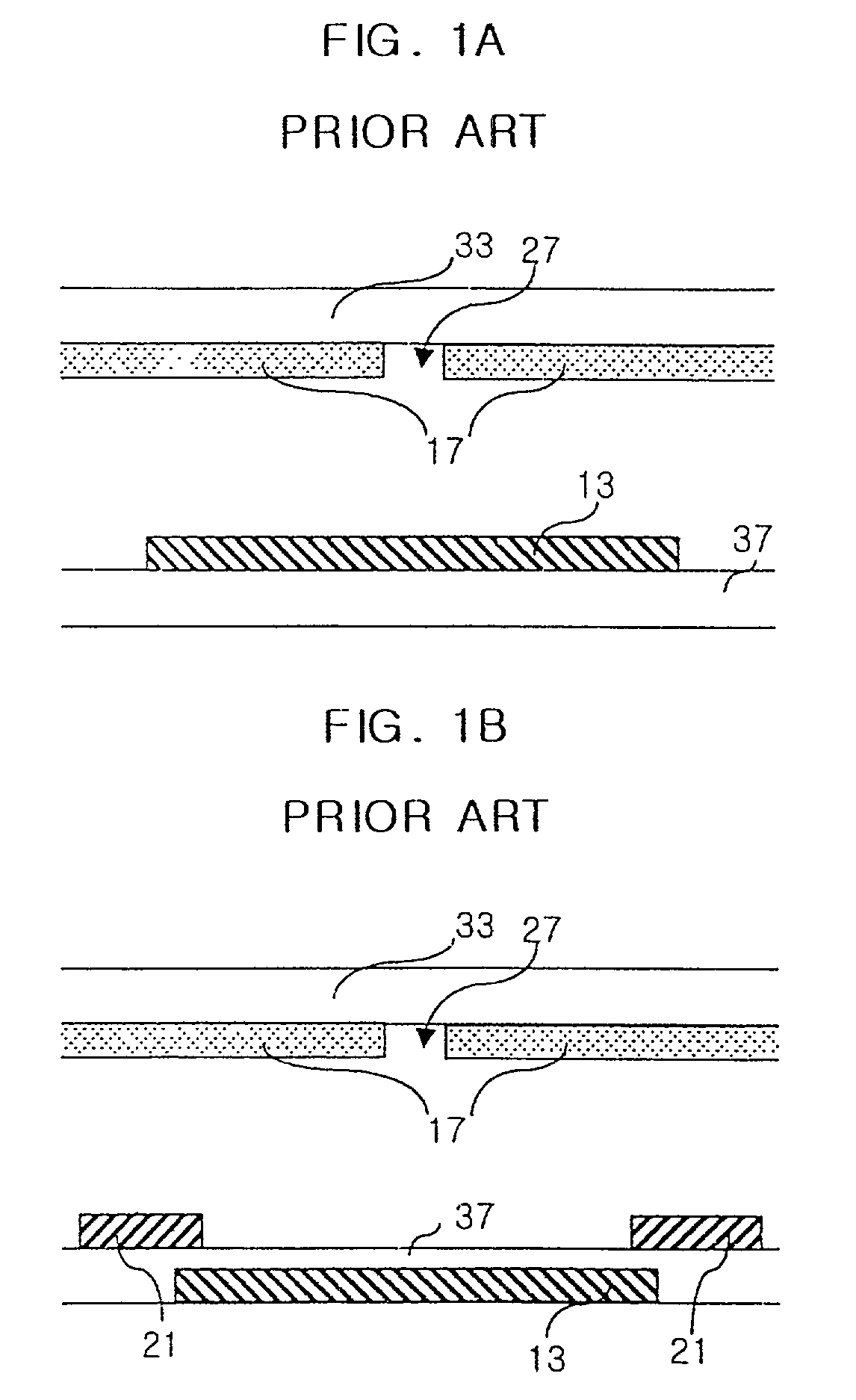
[0038]As shown in the figures, the present invention comprises first and second substrates 31, 33, a plurality of gate bus lines 1 arranged in a first direction on the first substrate and a plurality of data bus lines 3 arranged i...


PUM

PropertyMeasurementUnit
dielectric constantaaaaaaaaaa
electric fieldaaaaaaaaaa

Abstract

A multi-domain liquid crystal display device includes a liquid crystal layer between first and second substrates. A plurality of gate bus lines and data bus lines are arranged in a first and second direction, respectively, on the first substrate, to define a pixel region. A common-auxiliary electrode surrounds the pixel region on a same layer whereon the gate bus line is formed. A gate insulator and a passivation layer are formed over the whole first substrate. A pixel electrode, having an electric field inducing window in the inner part thereof, is formed in the pixel region. A light shielding layer is formed on the second substrate, a color filter is formed on the light shielding layer, a common electrode is formed on the color filter layer. An alignment layer is formed on at least one substrate between the first and second substrates.

Description

[0001]This application is a continuation of application Ser. No. 09 / 327,283 Filed on Jun. 4, 1999, now U.S. Pat. No. 6,462,798BACKGROUND OF THE INVENTION[0002]1. Field of the Invention[0003]The present invention relates to a liquid crystal display device (LCD), and more particularly, to a liquid crystal display device having common-auxiliary electrodes and electric field inducing windows.[0004]2. Description of the Related Art[0005]Recently, an LCD has been proposed where the liquid crystal is not aligned and the liquid crystal is driven by side electrodes insulated from pixel electrodes. FIGS. 1a and 1b are sectional views of pixel unit of the conventional LCDs.[0006]Regarding conventional LCDs, a plurality of gate bus lines arranged in a first direction on a first substrate and a plurality of data bus lines arranged in a second direction on the first substrate divide the first substrate into a plurality of pixel regions. A thin film transistor (TFT) applies image signal delivered ...

Claims


Application Information

Patent Timeline
Patent Type & Authority Patents(United States)
IPC IPC(8): G02F1/1343G02F1/1337G02F1/137G02F1/1333G02F1/1335G02F1/136G02F1/1368
CPCG02F1/133345G02F1/134336G02F1/133753G02F1/133707G02F1/1337G02F1/1343
Inventor KIM, KYEONG JINLEE, YUN BOKYOO, JANG JIN
Owner LG DISPLAY CO LTD
Why Eureka
Try Eureka