Multi-domain liquid crystal display device

a liquid crystal display and multi-domain technology, applied in non-linear optics, instruments, optics, etc., can solve the problems of weak electric field distortion needed to divide the pixel region, decrease in brightness, etc., and achieve high response time characteristics, stable arrangement of liquid crystal molecules, and high brightness

Inactive Publication Date: 2006-08-22
LG DISPLAY CO LTD
View PDF1 Cites 10 Cited by
  • Summary
  • Abstract
  • Description
  • Claims
  • Application Information

AI Technical Summary

Benefits of technology

[0012]An object of the present invention is to provide a multi-domain LCD having high response time characteristics and high brightness by stable arrangement of liquid crystal molecules, and preventing the flicker from generating.

Problems solved by technology

If the electrodes do not have an open area or the width of the open area is narrow, the electric field distortion needed to divide the pixel region becomes weak.
At this time, disclination occurs from the area where the liquid crystal directors are parallel with a transmittance axis of the polarizer, which results in a decrease in brightness.
Furthermore, in the conventional LCDs, although a storage electrode is formed on the gate bus line to maintain the voltage applied to the pixel electrode, there are still the problems of filters resulted from the shortage generated between the gate bus line and the storage electrode.

Method used


Image

  • Multi-domain liquid crystal display device
  • Multi-domain liquid crystal display device
  • Multi-domain liquid crystal display device

Examples


first embodiment

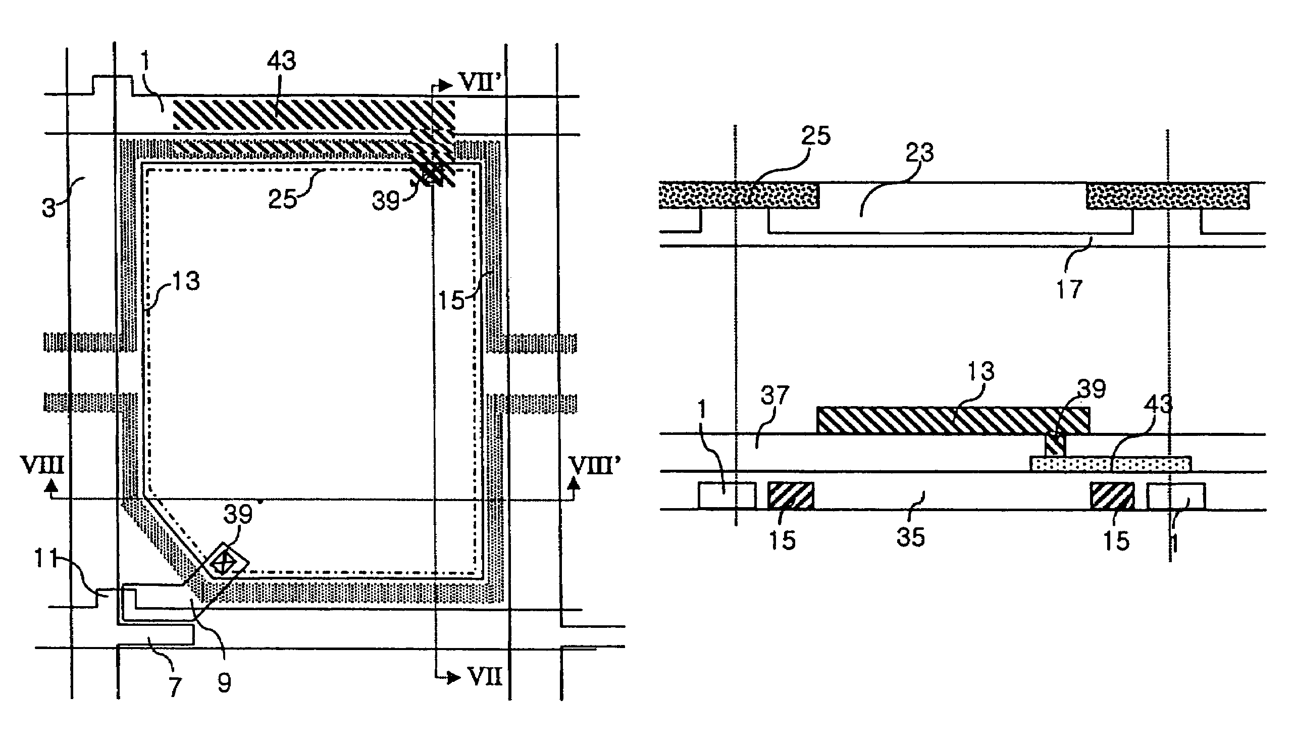
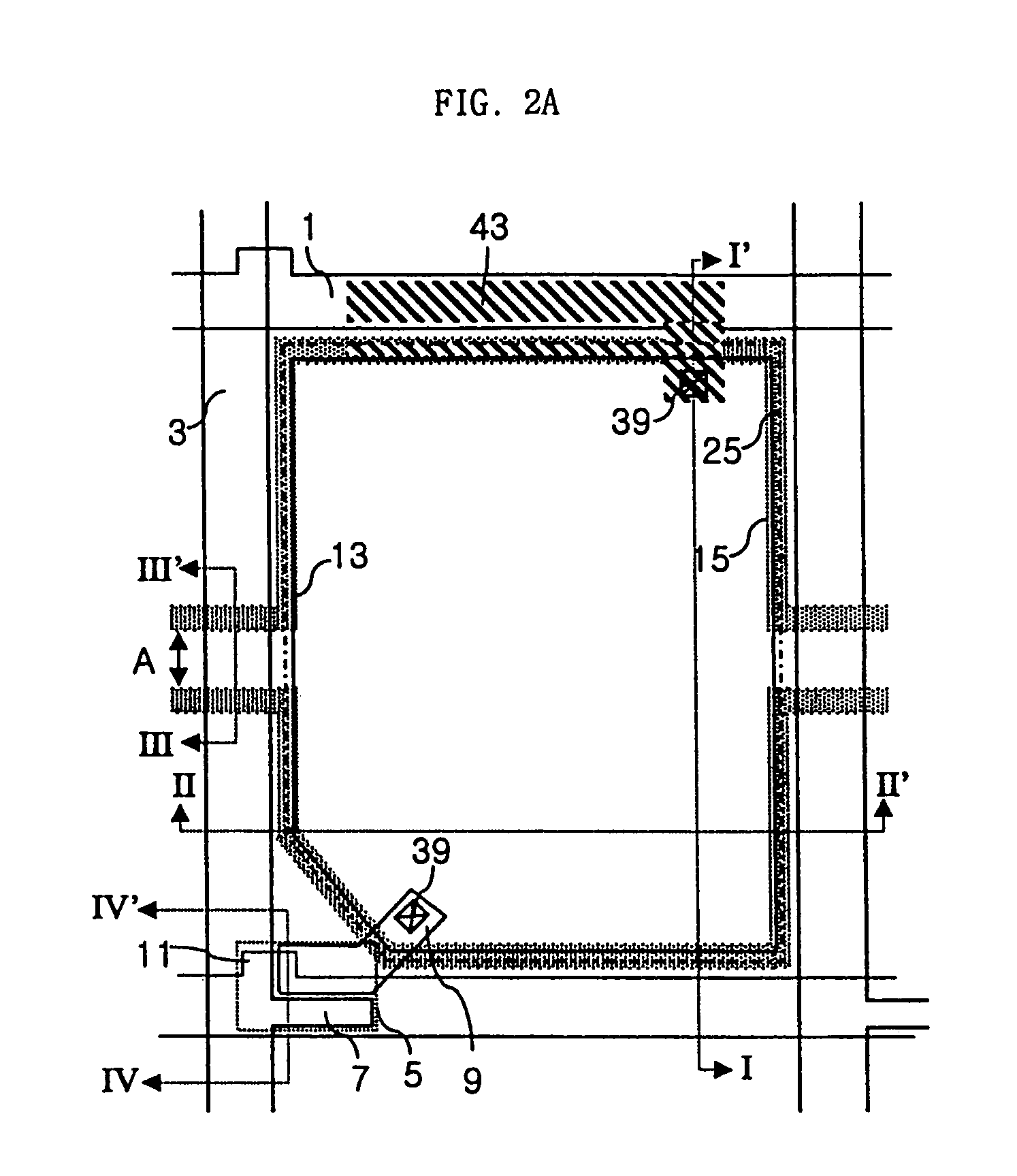
[0055]FIGS. 2A to 2C are plans of the multi-domain liquid crystal display devices according to the present invention, FIG. 3 is a sectional view taken along the line I—I of FIG. 2A, FIGS. 4A to 4B are sectional views taken along the line II—II of FIG. 2A, FIG. 5 is a sectional view taken along the line III—III of FIG. 2A, FIG. 6 is a sectional view taken along the line IV—IV of FIG. 2A, FIG. 7 is a sectional view taken along the line V—V of FIG. 2B.

[0056]As shown in the figures, the present invention comprises first and second substrates, a plurality of gate bus lines 1 arranged in a first direction on a first substrate and a plurality of data bus lines 3 arranged in a second direction on the first substrate, a common-auxiliary electrode 15, a TFT, a passivation layer 37, and a pixel electrode 13.

[0057]Data bus lines 3 and gate bus lines 1 divide the first substrate into a plurality of pixel regions. The common-auxiliary electrode 15 comprises at least one electrode in a pixel regio...

second embodiment

[0105]FIGS. 33A, 33B are plan views of the multi-domain liquid crystal display device according to the twenty-second embodiment of the present invention, FIGS. 33C, 33D are sectional views taken along the line III—III of FIG. 33B, and FIGS. 33E to 33H are sectional views taken along the line IV—IV of the FIG. 33A.

[0106]The pixel electrode 13 does not overlap common-auxiliary electrode 15, the light shielding layer 25 overlaps the common-auxiliary electrode 15, and the storage electrode 43 overlaps common-auxiliary electrode 15 and gate bus line 1 to forms a storage capacitance.

[0107]At this time, the gate insulator 35 and the passivation layer 37 on the common-auxiliary electrode 15 are removed, which intensifies the electric field of common-auxiliary electrode 15 that is applied to the pixel electrode 13.

[0108]The FIG. 33C shows a portion of the gate insulator 35 and passivation layer 37 that are removed to expose a part of the common-auxiliary electrode 15, and the FIG. 3D shows t...

third embodiment

[0110]FIGS. 34A and 34B are plan view and sectional view taken along the line V—V of FIG. 34A of the multi-domain liquid crystal display device according to the twenty-third embodiment of the present invention.

[0111]In this embodiment, a pair of upper-lower pixel regions co-owns one common-auxiliary electrode 15, and the storage electrodes 43 in the upper-lower pixel regions are formed on the common-auxiliary electrode 15, so that the aperture ratio is largely improved.

[0112]The pixel electrode 13 overlaps common-auxiliary electrode 15, the light shielding layer 25 overlaps the common-auxiliary electrode 15, and the storage electrode 43 overlaps common-auxiliary electrode 15 and gate bus line 1 to forms a storage capacitance.

[0113]In addition, in this embodiment it is possible to form the dielectric frame 53 on the common electrode 17 or the electric field inducing window 51 in the common electrode 17.


PUM

PropertyMeasurementUnit
response timeaaaaaaaaaa
distanceaaaaaaaaaa
distanceaaaaaaaaaa

Abstract

A multi-domain liquid crystal display device comprises first and second substrates facing each other; a liquid crystal layer between the first and second substrates; a plurality of gate bus lines arranged in a first direction on the first substrate and a plurality of data bus lines arranged in a second direction on the first substrate to define a plurality of pixel region; a thin film transistor positioned at a crossing area of the data bus line and the gate bus line, the thin film transistor comprising a gate electrode, a semiconductor layer, and source / drain electrodes; a common-auxiliary electrode comprising at least one electrode in the each pixel region; a plurality of pixel electrodes electrically charged through the thin film transistor; and an alignment layer on at least one substrate between the first and second substrates.

Description

CROSS REFERENCE TO RELATED APPLICATIONS[0001]This application is a divisional of prior application Ser. No. 09 / 598,213, filed Jun. 21, 2000, now U.S. Pat. No. 6,791,647 which is a Continuation-in-Part of U.S. patent application Ser. No. 09 / 256,180 filed on Feb. 24, 1999, now U.S. Pat. No. 6,809,787, and this application also claims the benefit of Korean Patent Application No. 1999-23194, filed on Jun. 21, 1999 and No. 1999-32945, filed on Aug. 11, 1999, which are hereby incorporated by reference for all purposed as if fully set forth herein.BACKGROUND OF THE INVENTION[0002]1. Field of the Invention[0003]The present invention relates to a liquid crystal display device (LCD), and more particularly, to a liquid crystal display device having a common-auxiliary electrode.[0004]2. Description of the Related Art[0005]Recently, an LCD has been proposed where the liquid crystal is not aligned and the liquid crystal is driven by side-electrodes insulated from pixel electrodes. FIG. 1 is secti...

Claims


Application Information

Patent Timeline
Patent Type & Authority Patents(United States)
IPC IPC(8): G02F1/1337G02F1/1343G02F1/1362
CPCG02F1/136213G02F1/136286G02F2001/136218G02F1/136218
Inventor KIM, JEOM JAEKO, DOO HYUNLEE, JOUN HOKIM, JONG SOONKIM, JONG HWANCHO, YOUNG WOOCHU, MI KYUNG
Owner LG DISPLAY CO LTD
Why Eureka
Try Eureka