

Multi-domain liquid crystal display device
a liquid crystal display and multi-domain technology, applied in static indicating devices, instruments, non-linear optics, etc., can solve the problems of weak electric field distortion needed to divide the pixel region, decrease in brightness, etc., and achieve high response time characteristics, stable arrangement of liquid crystal molecules, and high brightness
- Summary
- Abstract
- Description
- Claims
- Application Information
AI Technical Summary
Benefits of technology
Problems solved by technology
Method used
Image

Examples
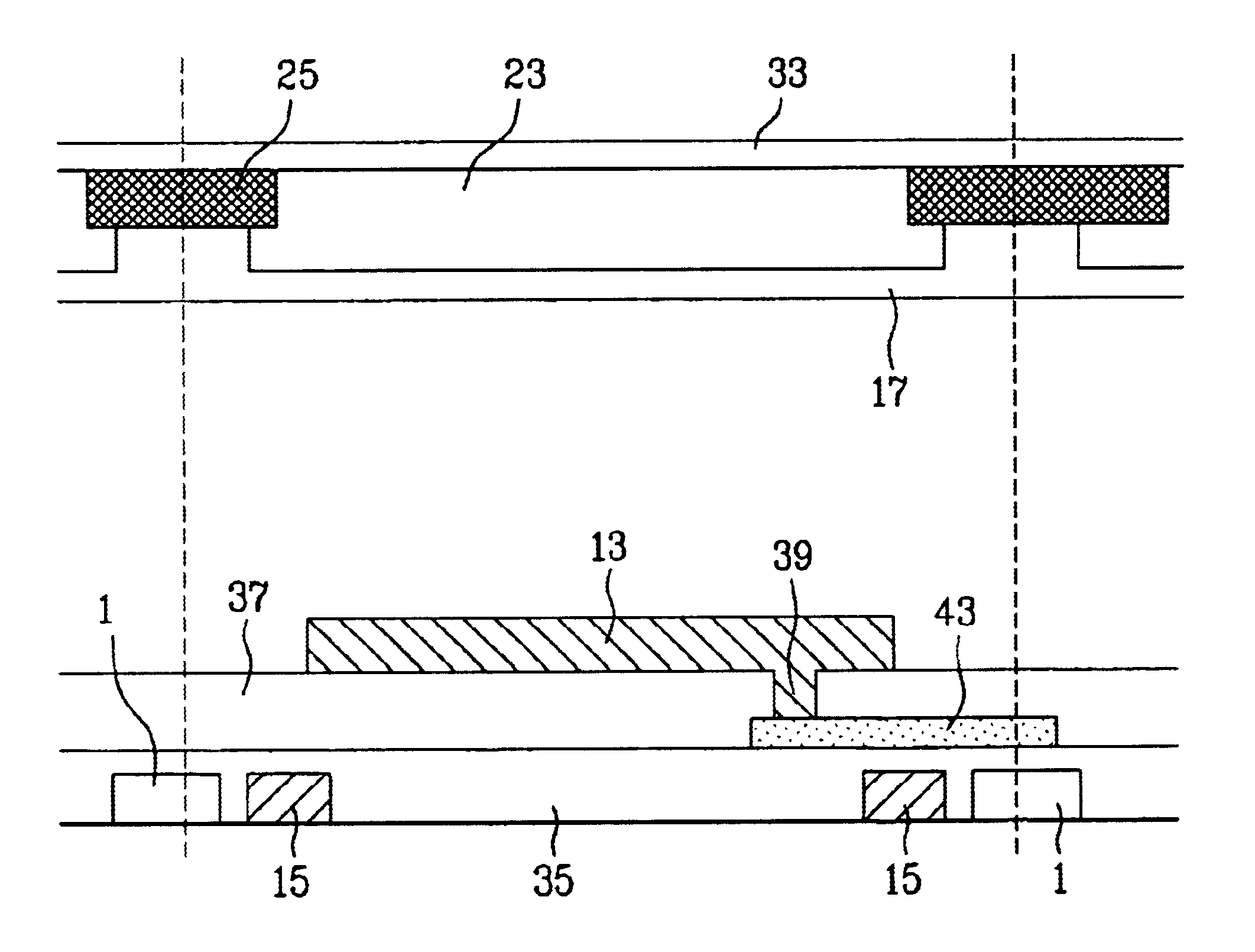
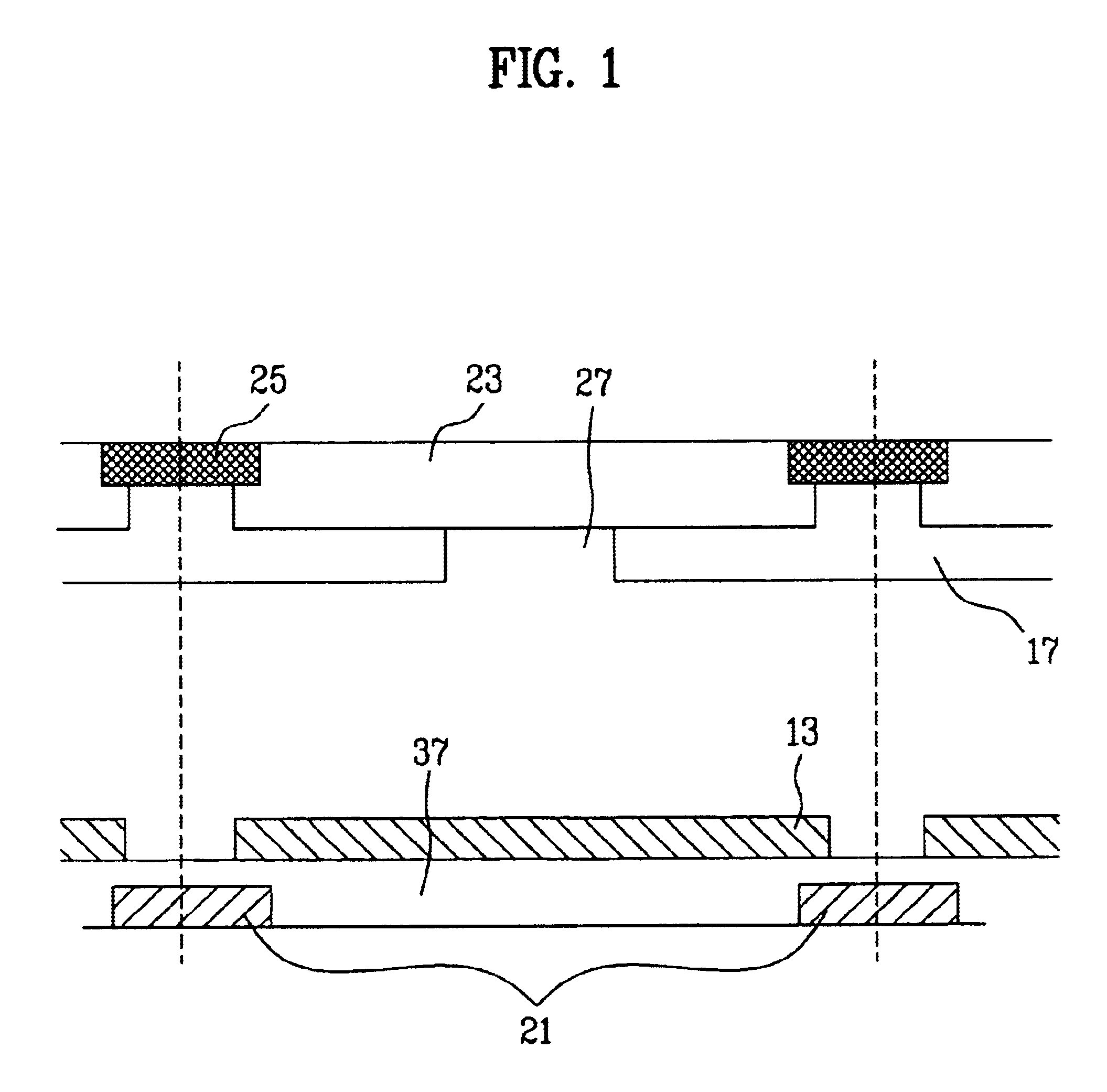
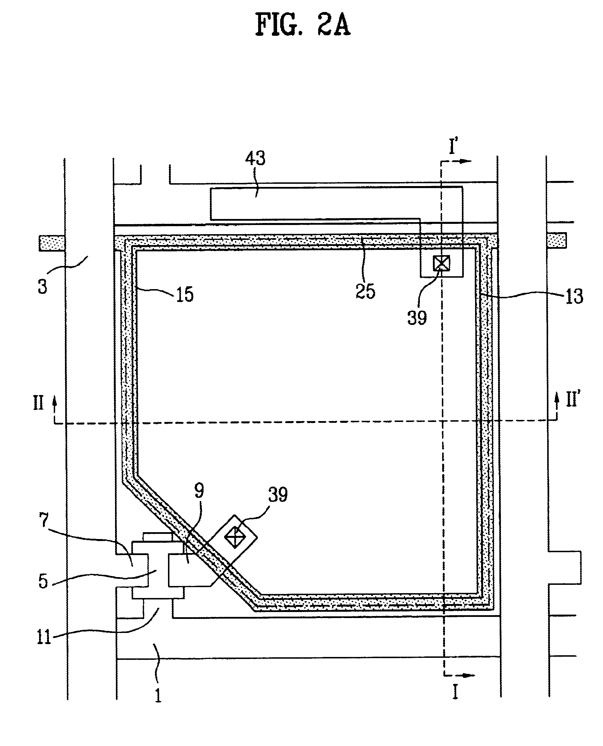
first embodiment
FIGS. 2A and 2B are plan views of the multi-domain liquid crystal display devices according to the present invention, and FIGS. 2C and 2D, 2E, 2F, 2G are sectional views taken along the lines I-I' and II-II' in FIG. 2A.
As shown in the figures, the present invention comprises first and second substrates, a plurality of gate bus lines 1 arranged in a first direction on a first substrate and a plurality of data bus lines 3 arranged in a second direction on the first substrate, a common-auxiliary electrode 15, a TFT, a passivation layer 37, and a pixel electrode 13.
On a second substrate, a light shielding layer 25 is formed to shield the light leaked from gate and data bus lines 1, 3, and the TFT, a color filter layer 23 is formed on the light shielding layer, a common electrode 17 is formed on the color filter layer, and a liquid crystal layer is formed between the first and second substrates.
Data bus lines 3 and gate bus lines 1 divide the first substrate into a plurality of pixel reg...
second embodiment
FIGS. 3A and 3B are plan views of the multi-domain liquid crystal display devices according to the present invention, and FIGS. 3C and 3D are sectional views taken along the lines III-III' in FIG. 3B, FIGS. 3E, 3F, 3G, 3H are sectional views taken along the lines IV-IV' in FIG. 3A.
Pixel electrode 13 does not overlap common-auxiliary electrode 15, and the light shielding layer 25 overlaps the pixel electrode 13. At this time, the gate insulator 35 and the passivation layer 37 on the common-auxiliary electrode 15 are removed, which intensifies the electric field of common-auxiliary electrode 15 that is applied to the pixel electrode 13 (refer to FIG. 3B).
The FIG. 3C shows a portion of the gate insulator 35 and passivation layer 37 that are removed to expose a part of the common-auxiliary electrode 15, and the FIG. 3D shows that three sides of the common-auxiliary electrode 15 are exposed.
Storage electrode 43 forms storage capacitor by overlapping gate bus line 1. Although not shown in...
third embodiment
FIG. 4A is a plan view of the multi-domain liquid crystal display device according to the present invention, and FIGS. 4B and 4C, 4D, 4E, 4F are sectional views taken along the lines V-V' and VI-VI' in FIG. 4A.
In the multi-domain LCD of the present invention, a part of upper-down pixels is formed on common-auxiliary electrode 15 that include a storage electrode 43. The aperture ratio is largely improved as compared to the LCD in FIG. 2.
Moreover, the pixel electrode 13 overlaps common-auxiliary electrode 15, the light shielding layer 25 overlaps the common-auxiliary electrode 15, and the storage electrode 43 forms a storage capacitor with common-auxiliary electrode 15. FIGS. 4C, 4D show that dielectric frame 53 is formed on the common electrode 17, and FIGS. 4E, 4F show that electric field inducing window 51 is formed in the common electrode 17. Also, FIGS. 4D, 4F show that the light shield layer 25 is formed only on the thin film transistor.
PUM
| Property | Measurement | Unit |
|---|---|---|
| response time | aaaaa | aaaaa |
| electric field | aaaaa | aaaaa |
| dielectric anisotropy | aaaaa | aaaaa |
Abstract
Description
Claims
Application Information