
Diode array architecture for addressing nanoscale resistive memory arrays

a resistive memory array and diode array technology, applied in the field of memory devices, can solve problems such as the breakdown of diodes

Active Publication Date: 2006-04-25
MONTEREY RES LLC
View PDF1 Cites 109 Cited by
  • Summary
  • Abstract
  • Description
  • Claims
  • Application Information

AI Technical Summary

Problems solved by technology

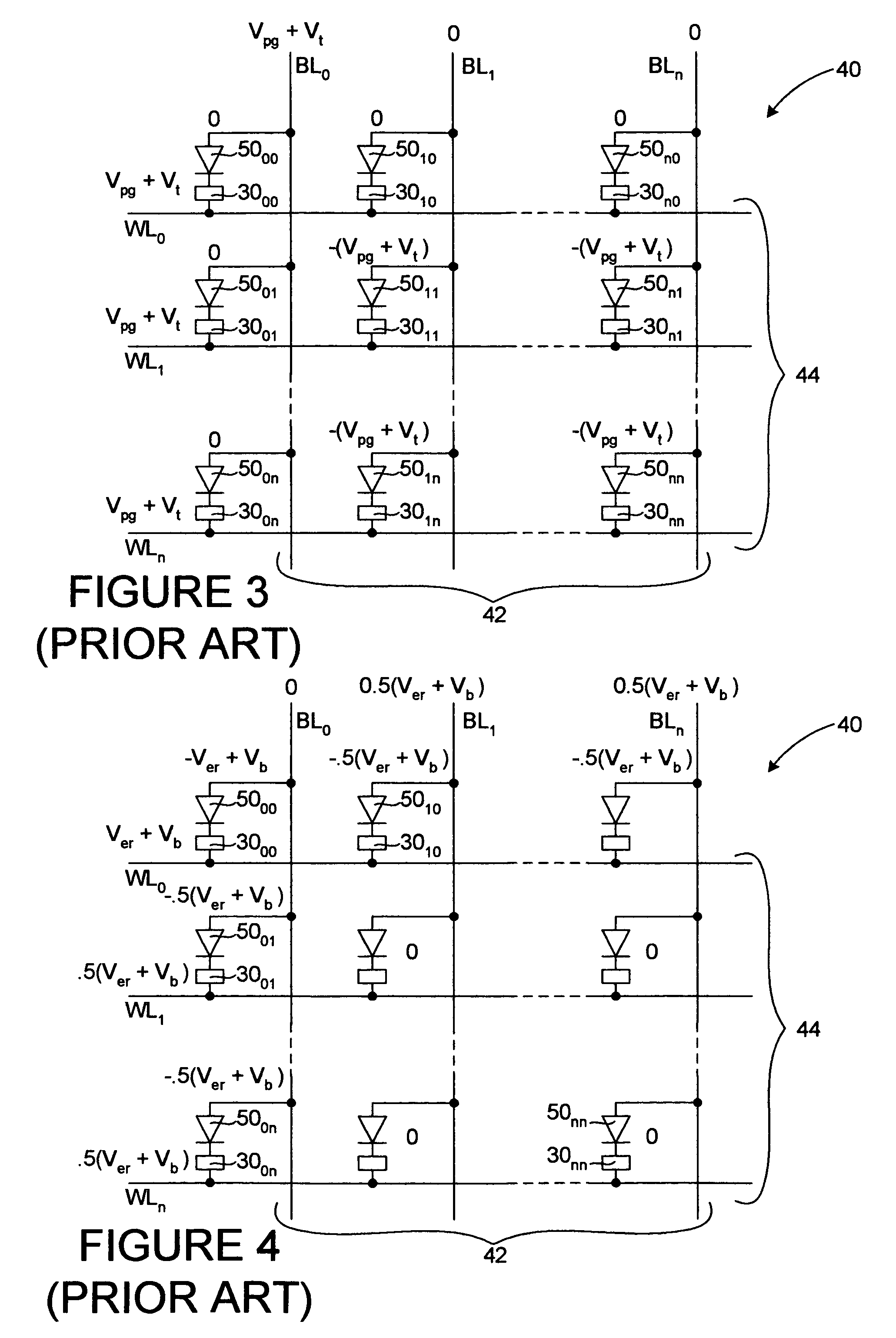
This leads to problems in achieving breakdown of the diode, which is essential in erasing the associated memory cell as described above.

Method used


Image

  • Diode array architecture for addressing nanoscale resistive memory arrays
  • Diode array architecture for addressing nanoscale resistive memory arrays
  • Diode array architecture for addressing nanoscale resistive memory arrays

Examples


Embodiment Construction

[0029]Reference is now made in detail to a specific embodiment of the present invention which illustrates the best mode presently contemplated by the inventors for practicing the invention.

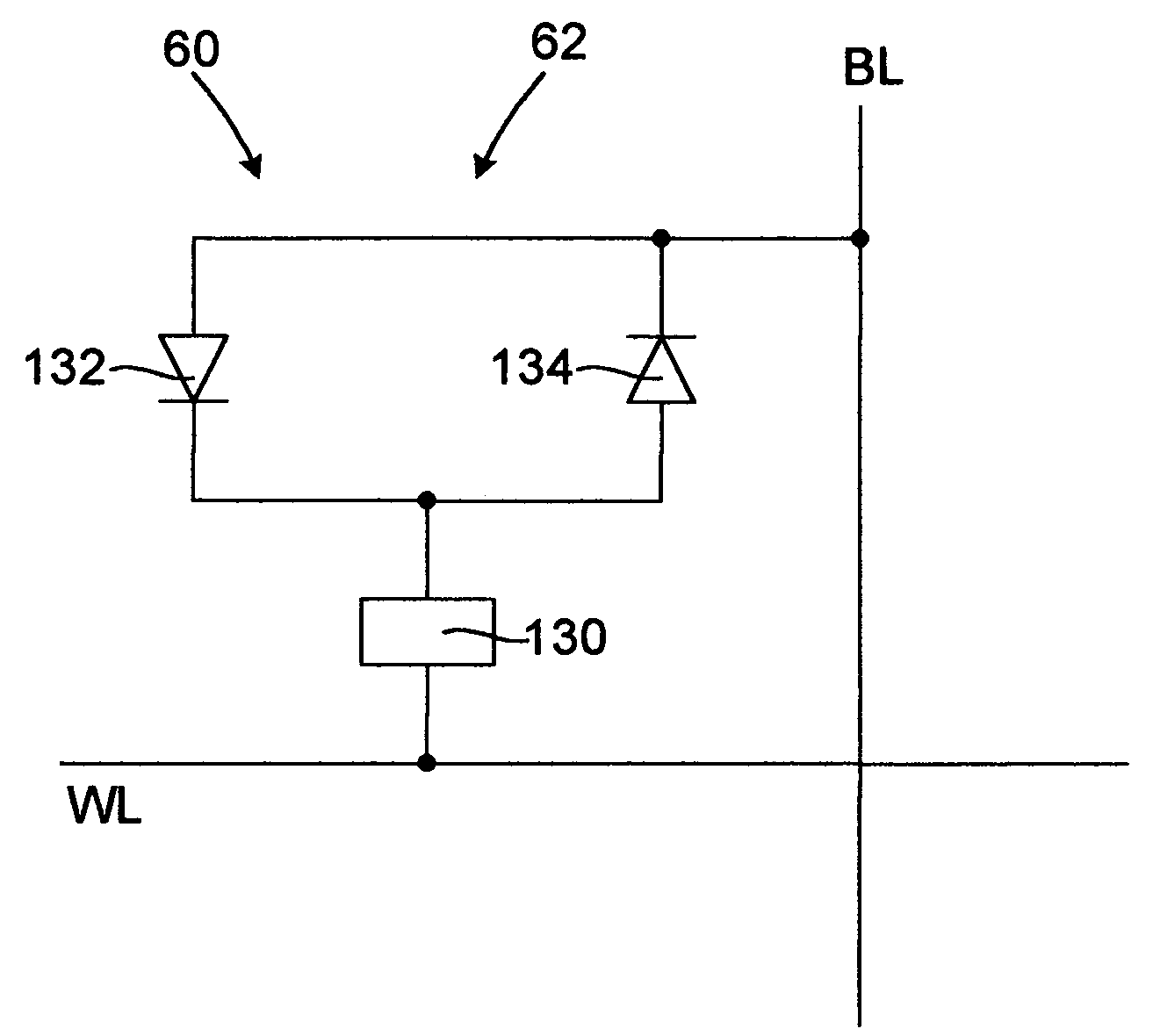
[0030]FIG. 7 illustrates an embodiment of the present invention. A conductor BL is shown therein, and a conductor WL overlies, crosses and is spaced from the conductor BL. A structure 60 interconnects the conductor BL and the conductor WL at the intersection thereof. The structure 60 includes a resistive memory cell 130, similar to the resistive memory cell 30 above, connected to the conductor WL, a first diode 132 connected to the resistive memory cell 130 and the conductor BL, and a second diode 134 also connected to the resistive memory cell 130 and the conductor BL, in parallel with the first diode 132. The first diode 132 is oriented in the forward direction from the resistive memory cell 130 to the conductor BL, and the second diode 134 is oriented in the reverse direction from the resistive...


PUM


Abstract

The present memory structure includes thereof a first conductor, a second conductor, a resistive memory cell connected to the second conductor, a first diode connected to the resistive memory cell and the first conductor, and oriented in the forward direction from the resistive memory cell to the first conductor, and a second diode connected to the resistive memory cell and the first conductor, in parallel with the first diode, and oriented in the reverse direction from the resistive memory cell to the first conductor. The first and second diodes have different threshold voltages.

Description

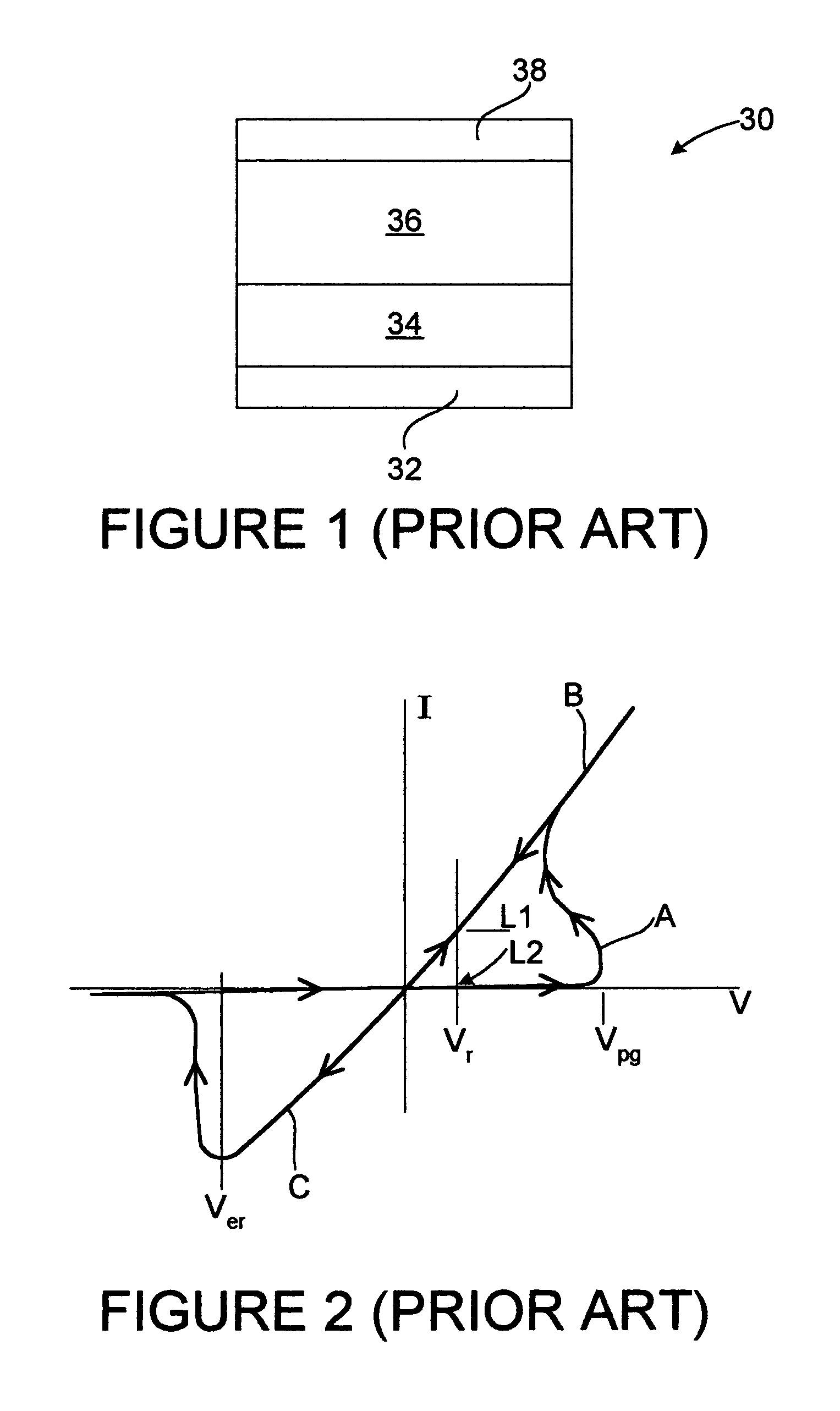
BACKGROUND OF THE INVENTION[0001]1. Technical Field[0002]This invention relates generally to memory devices, and more particularly, to a memory array incorporating resistive memory cells.[0003]2. Background Art[0004]Generally, memory devices associated with computers and other electronic devices are employed to store and maintain information for the operation thereof. Typically, such a memory device includes an array of memory cells, wherein each memory cell can be accessed for programming, erasing, and reading thereof. Each memory cell maintains information in an “off” state or an “on” state, also referred to as “0” and “1” respectively, which can be read during the reading step of that memory cell.[0005]As such electronic devices continue to be developed and improved, the amount of information required to be stored and maintained continues to increase. FIG. 1 illustrates a type of memory cell known as a nanoscale resistive memory cell 30, which includes advantageous characteristic...

Claims


Application Information

Patent Timeline
Patent Type & Authority Patents(United States)
IPC IPC(8): G11C11/36G11C27/00
CPCG11C13/0002G11C13/0007G11C13/003H01L27/1021H01L27/101G11C2213/56G11C2213/74G11C2213/76G11C2213/72
Inventor TRIPSAS, NICHOLAS H.BILL, COLIN S.VANBUSKIRK, MICHAEL A.BUYNOSKI, MATTHEWFANG, TZU-NINGCAI, WEI DAISYPANGRLE, SUZETTEAVANZINO, STEVEN
Owner MONTEREY RES LLC
Learn More