High speed and high precision sensing for digital multilevel non-volatile memory system

a non-volatile memory system, high-speed technology, applied in static storage, digital storage, instruments, etc., can solve the problems of low impedance driver stage driving a heavy and noisy load, and achieve high-speed load, wide output range, and low impedance

Active Publication Date: 2006-05-02
SILICON STORAGE TECHNOLOGY
View PDF10 Cites 40 Cited by
  • Summary
  • Abstract
  • Description
  • Claims
  • Application Information

AI Technical Summary

Problems solved by technology

The low impedance driver stage may drive a heavy and noisy load.

Method used


Image

  • High speed and high precision sensing for digital multilevel non-volatile memory system
  • High speed and high precision sensing for digital multilevel non-volatile memory system
  • High speed and high precision sensing for digital multilevel non-volatile memory system

Examples


Embodiment Construction

[0023]As used herein, “data cell” refers to the regular data memory cells, “reference cell” refers to memory cells being used as to generate reference levels for sensing, “redundant cell” refers to memory cells being used to replace defective data cells.

[0024]As used herein, a N-type NMOS enhancement transistor is an enhancement transistor having a gate threshold, for example in the range of approximately 0.3 to 1.0 volts. A P-type transistor is a PMOS enhancement transistor having a gate threshold approximately in the range of −0.3 to −1.0 volts. An NZ NMOS transistor is a native low voltage transistor having a gate threshold approximately in the range of −0.1 to 0.2 volts.

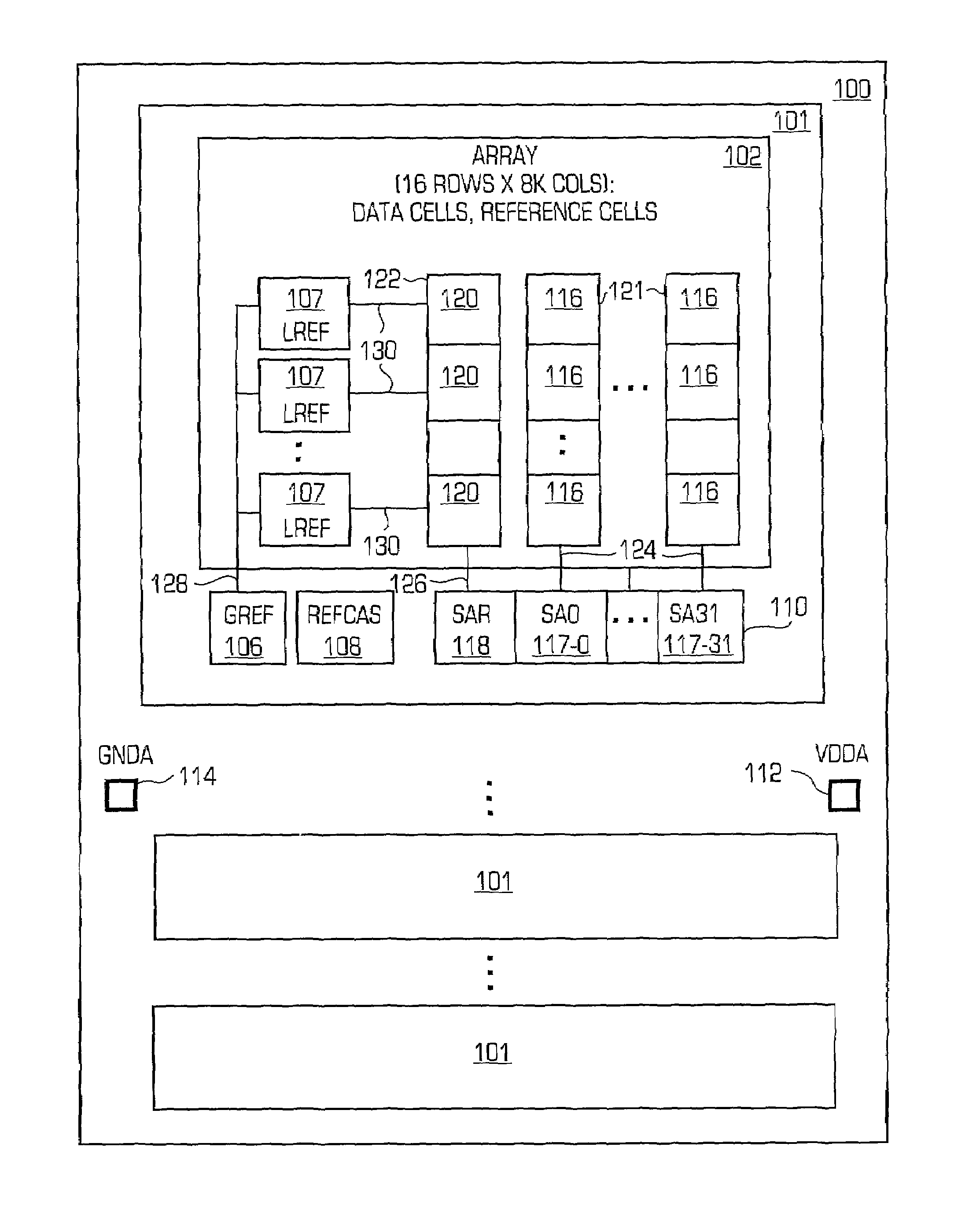
[0025]FIG. 1 is a block diagram illustrating a non-volatile multilevel memory system 100.

[0026]The non-volatile multilevel memory system 100 comprises a plurality of arrays 101. (For clarity, only three arrays 101 are shown, and the details of only one array 101 is shown.) Each array 101 comprises a memory array ...


PUM


Abstract

A digital multilevel non-volatile memory includes a massive sensing system that includes a plurality of sense amplifiers disposed adjacent subarrays of memory cells. The sense amplifier includes a high speed load, a wide output range intermediate stage and a low impedance output driver. The high speed load provides high speed sensing. The wide output range provides a sensing margin at high speed on the comparison node. The low impedance output driver drives a heavy noisy load of a differential comparator. A precharge circuit coupled to the input and output of the sense amplifier increases the speed of sensing. A differential comparator has an architecture that includes analog bootstrap. A reference sense amplifier has the same architecture as the differential amplifier to reduce errors in offset. The reference differential amplifier also includes a signal multiplexing for detecting the contents of redundant cells and reference cells.

Description

CROSS REFERENCE TO RELATED APPLICATIONS[0001]This application is related to U.S. patent application Ser. No. 10 / 241,266, filed on even date herewith, entitled “Differential Sense Amplifier For Multilevel Non-Volatile Memory”, inventors Hieu Van Tran, Jack Edward Frayer, William John Saiki, and Michael Stephen Briner, the disclosure of which is incorporated herein by reference.BACKGROUND OF THE INVENTION[0002]As information technology progresses at an unprecedented pace, the need for information storage increases proportionately. Accordingly, the non-volatile information in stationary or portable communication demands higher capability and capacity storage. One approach to increasing the amount of storage is by decreasing physical dimensions of the stored bit (e.g., memory cell) to smaller dimensions, such as the nano cell technology. Another approach is to increase the stored density per bit. This second approach is known as digital multilevel non-volatile storage technology.[0003]A...

Claims


Application Information

Patent Timeline
Patent Type & Authority Patents(United States)
IPC IPC(8): G11C7/00G11C11/56G11C16/28
CPCG11C11/5642G11C7/06G11C16/28
Inventor TRAN, HIEU VANFRAYER, JACK EDWARDSAIKI, WILLIAM JOHNBRINER, MICHAEL STEPHEN
Owner SILICON STORAGE TECHNOLOGY
Why Eureka
Try Eureka