Pattern inspection method

a technology of pattern inspection and inspection method, applied in the direction of material analysis using wave/particle radiation, instruments, etc., can solve the problems of inability to provide a method of inspection, inability to inspect the characteristic of the transistor, and inability to provide a technique, so as to achieve the effect of accurately estimating the electrical characteristics of the transistor

Inactive Publication Date: 2006-05-23
HITACHI LTD +1
View PDF5 Cites 59 Cited by
  • Summary
  • Abstract
  • Description
  • Claims
  • Application Information

AI Technical Summary

Benefits of technology

[0036]According to aspects (6), (7), (8), (9), and (10), it is possible to estimate a variation of the transistor's final gate length and highly accur

Problems solved by technology

The methods described in the above-mentioned patent documents 2 and 3 cannot provide a method of inspecting the roughness that varies with an area length or a measurement location.
Since the former example gives no consideration to the contribution of the portions in which the gate length is shorter than Lg−ΔLg, however, there may be an incapability of in

Method used


Image

  • Pattern inspection method
  • Pattern inspection method
  • Pattern inspection method

Examples


working examples

[0116]The following describes working examples of the pattern inspection system and method for implementing the above-mentioned embodiments in further detail with reference to the accompanying drawings.

working example 1

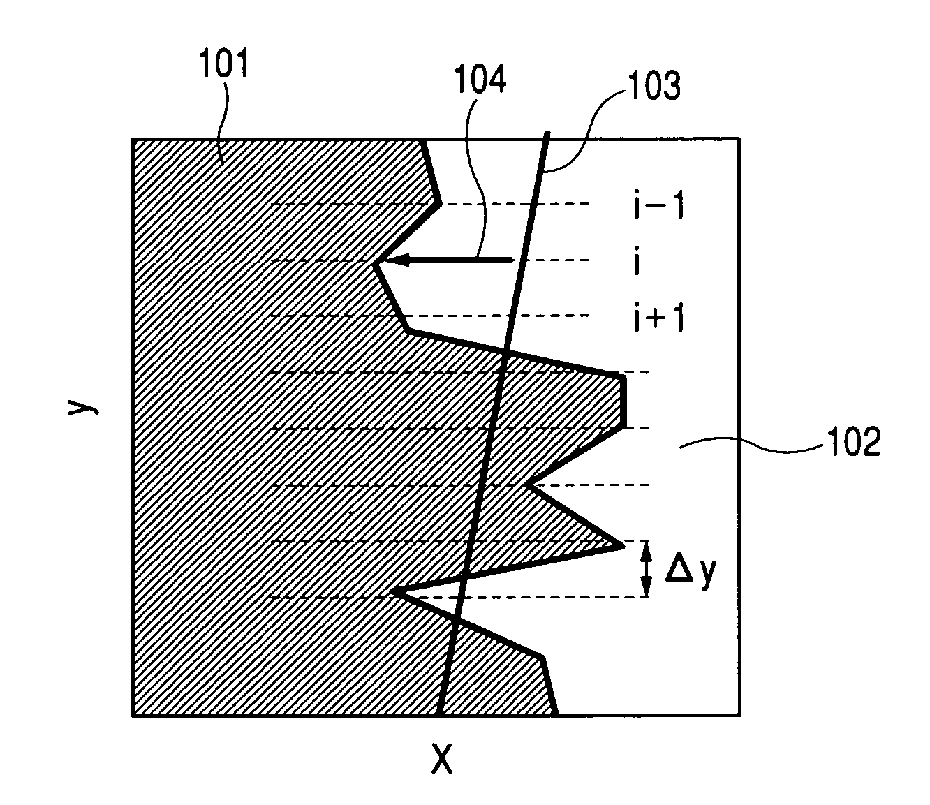
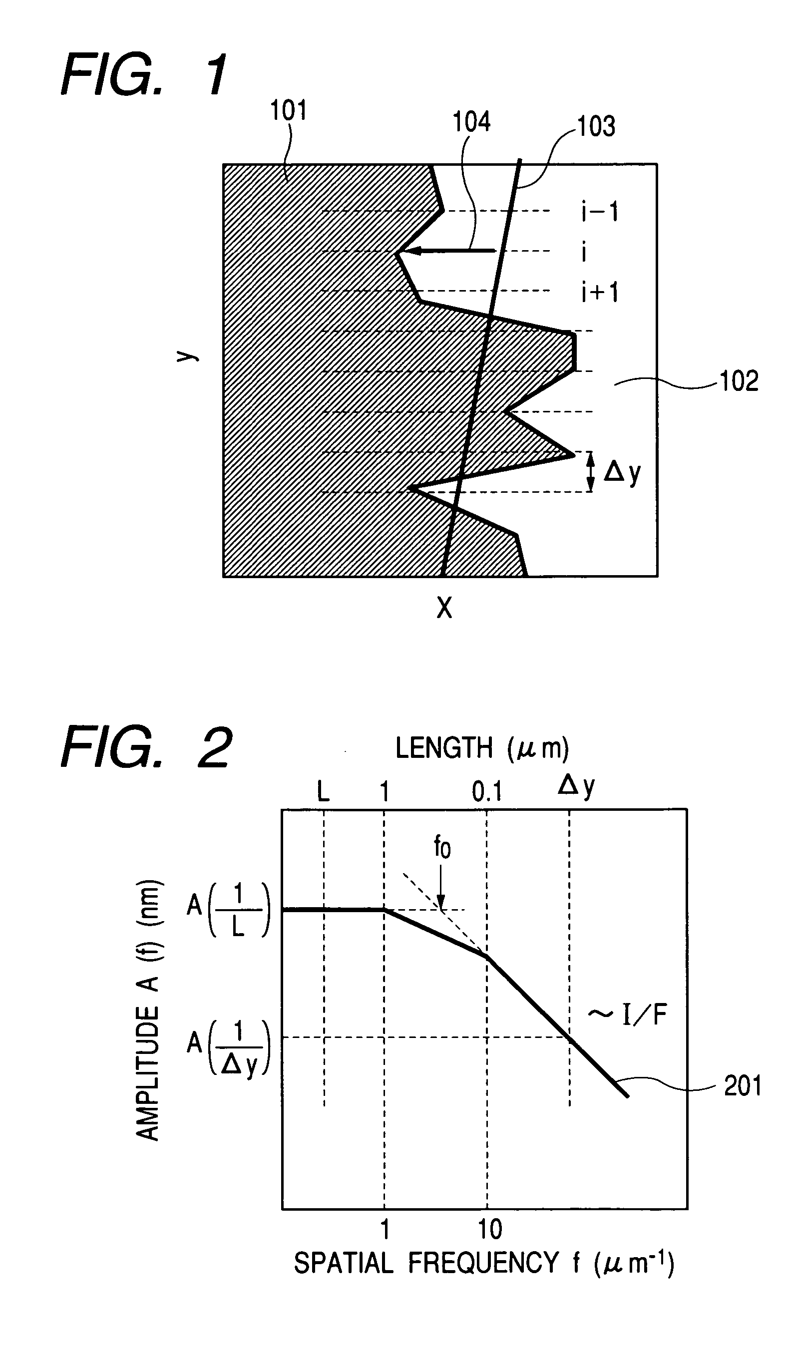
[0117]FIG. 7 is a pattern diagram showing an image observed by a scanning electron microscope. FIG. 8 is a flowchart showing a procedure of working example 1.

[0118]Working example 1 describes an example of calculating a line width variation from an SEM image that is obtained for the line pattern with a specified accuracy by using the present invention.

[0119]Working example 1 inspects a line pattern comprising a polycrystalline silicon corresponding to the transistor gate. In terms of designed sizes, the gate is 80 nm long and 0.6 μm wide. It is desirable that the actual gate width equals the length of a line in an inspection area for measuring the line width variation. For this purpose, the length of the observation area in the line direction is approximated to the gate width within a possible range. When the scanning electron microscope used for working example 1 is set to a magnifying power of two hundred thousands for observation, the visual field has the vertical size of 675 mm....

working example 2

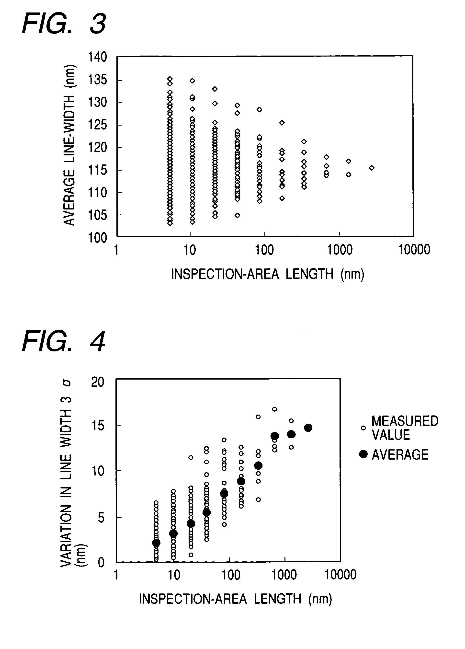
[0127]Working example 2 of the present invention will be described with reference to the above-mentioned flowchart in FIG. 8.

[0128]Working example 2 describes an example of finding a standard deviation for the line width distribution with respect to a long area of 1 μm or more from an SEM image that is obtained for the line pattern with a specified accuracy by using the present invention.

[0129]Similarly to working example 1, working example 2 inspects a line pattern comprising a polycrystalline silicon corresponding to the transistor gate. In terms of designed sizes, the gate is 80 nm long and 2 μm wide. It is desirable that the actual gate width equals the length of a line in an inspection area for measuring the line width variation. The length of the observation area in the line direction should preferably be approximated to the gate width within a possible range. It is also desirable to approximate the length of the observation area in the line direction to 5 μm. For this purpose...


PUM


Abstract

The present invention may include a pattern inspection method of extracting a pattern edge shape from an image obtained by a scanning microscope and inspecting the pattern. A control section and a computer of the scanning microscope process the intensity distribution of reflected electrons or secondary electrons, find the distribution of gate lengths in a single gate from data about edge positions, estimate the transistor performance by assuming a finally fabricated transistor to be a parallel connection of a plurality of transistors having various gate lengths, and determine the pattern quality and grade based on an estimated result. In this manner, it is possible to highly, accurately and quickly estimate an effect of edge roughness on the device performance and highly accurately and efficiently inspect patterns in accordance with device specifications.

Description

PRIORITY CLAIM[0001]This application claims priority under 35 U.S.C. §119 to Japanese patent application P2003-042116 filed Feb. 20, 2003, the entire disclosure of which is hereby incorporated herein by reference.FIELD OF THE INVENTION[0002]The present invention relates to a pattern inspection method and more particularly to a method of inspecting shapes of fine patterns formed on a semiconductor substrate by means of non-destructive measurements using a scanning microscope and detailed dimension measurements using an image process.BACKGROUND OF THE INVENTION[0003]For example, the inventors examined the following technologies associated with a method for inspecting fine patterns formed on a semiconductor substrate.[0004]In accordance with a recent tendency toward fine semiconductor device structures, careful consideration is being given to distribution of essential pattern sizes due to the presence of edge roughness, i.e., unevenness along edges of a fine pattern formed on a semicon...

Claims


Application Information

Patent Timeline
IPC IPC(8): G01N23/00G01B15/00G01B15/04G01B15/08
CPCG01B15/08G01B15/04
Inventor YAMAGUCHI, ATSUKOFUKUDA, HIROSHITSUCHIYA, RYUTAKAWADA, HIROKIYONEDA, SHOZO
Owner HITACHI LTD
Why Eureka
Try Eureka