Reticle design inspection system
- Summary
- Abstract
- Description
- Claims
- Application Information
AI Technical Summary
Benefits of technology
Problems solved by technology
Method used
Image

Examples
Embodiment Construction
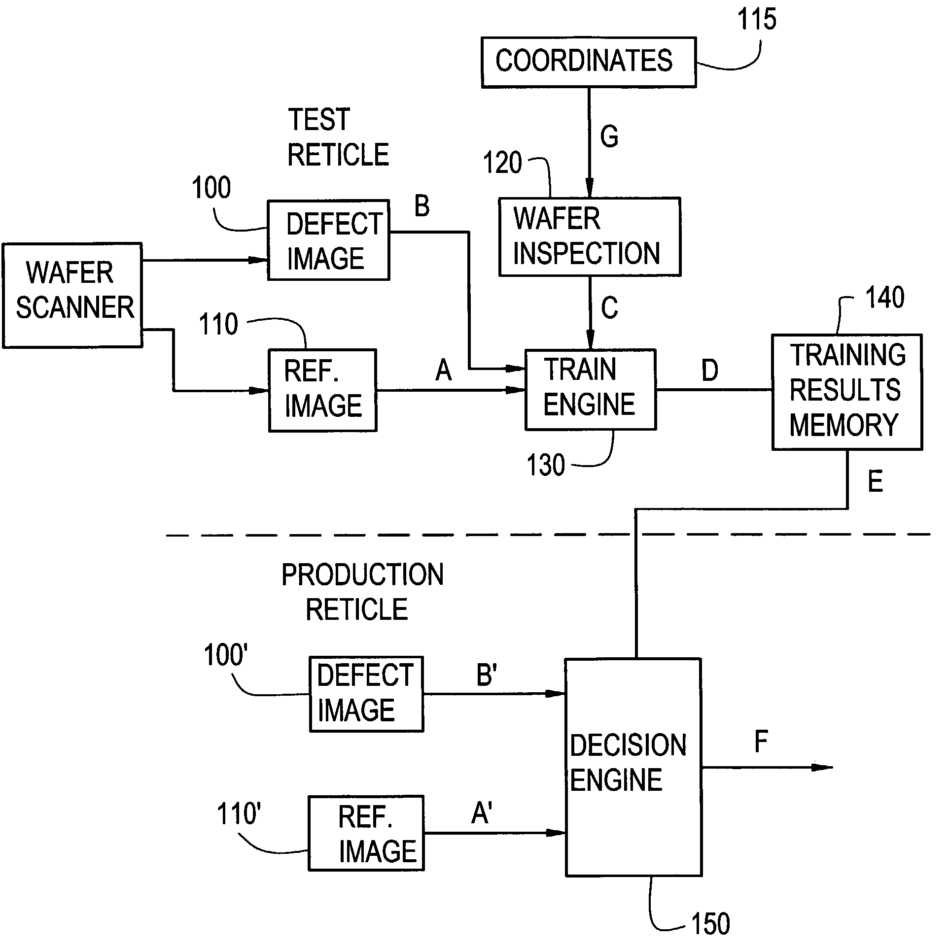
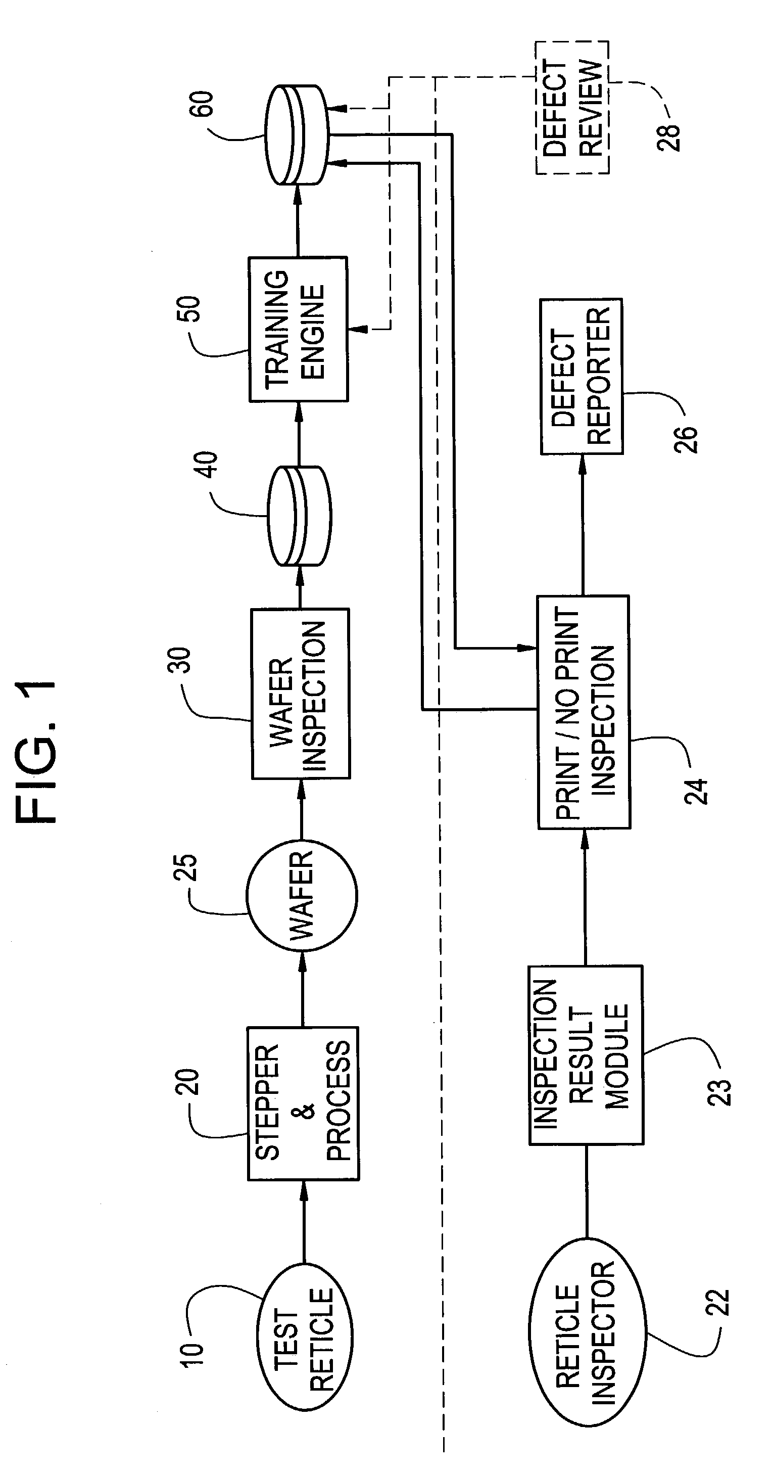
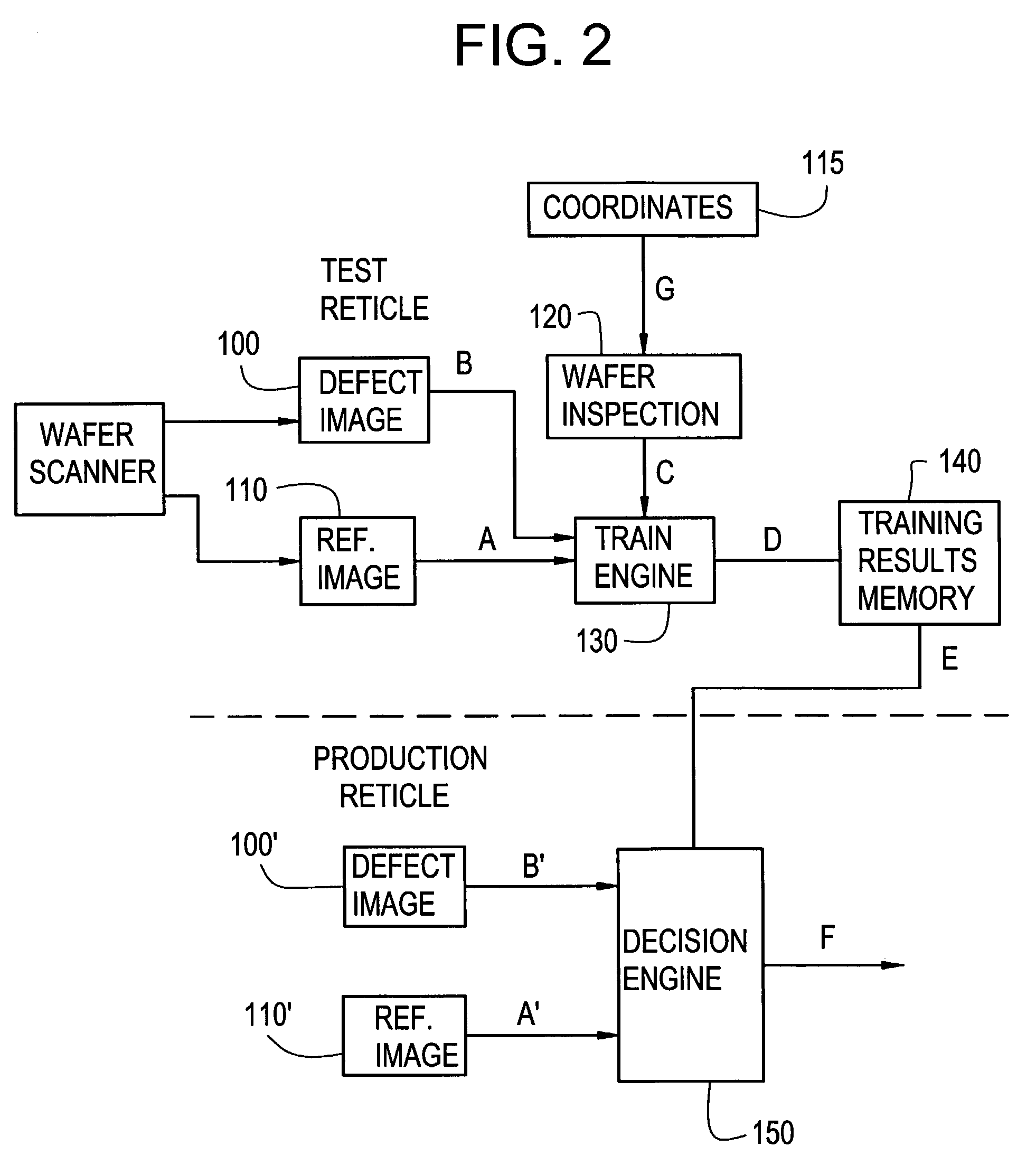
[0072]In accordance with a preferred embodiment of the invention, a reticle inspection system is trained to recognize which “pattern features” in a reticle transfer to a wafer as unacceptable defects during its manufacture and which do not so transfer. As noted above, the term “pattern-features” is a short hand to signify either or both of “design features” and “test defects.”FIG. 3 exemplifies a test mask / reticle substrate 300 which includes both design features and test defects. For example, design feature 310 is a 90° curved conductor line, design feature 320 (not shown) are contact holes of various sizes, design features 330 are isolated lines of various thickness, and design features 340 are grouped lines of various thickness. Similarly, design features 350 are various OPC features. On the other hand, test defects 315 are missing patterns, test defects 325 are extra patterns, test defects 335 are broken contacts of various sizes, and test defects 345 may be either an isolated e...
PUM
| Property | Measurement | Unit |
|---|---|---|
| widths | aaaaa | aaaaa |
| widths | aaaaa | aaaaa |
| widths | aaaaa | aaaaa |
Abstract
Description
Claims
Application Information
 - R&D
- Intellectual Property
- Life Sciences
- Materials
- Tech Scout
- Unparalleled Data Quality
- Higher Quality Content
- 60% Fewer Hallucinations
Browse by: Latest US Patents, China's latest patents, Technical Efficacy Thesaurus, Application Domain, Technology Topic, Popular Technical Reports.
© 2025 PatSnap. All rights reserved.Legal|Privacy policy|Modern Slavery Act Transparency Statement|Sitemap|About US| Contact US: help@patsnap.com