Apparatus and method for electrochemically depositing metal on a semiconductor workpiece
What is AI technical title?
AI technical title is built by Patsnap AI team. It summarizes the technical point description of the patent document.
a technology of electrochemical depositing and workpieces, applied in the direction of cell components, superimposed coating processes, transportation and packaging, etc., can solve the problems of general unsuitability for bulk electrolytic deposition
Inactive Publication Date: 2006-10-03
SEMITOOL INC
View PDF457 Cites 15 Cited by
Summary
Abstract
Description
Claims
Application Information
AI Technical Summary
This helps you quickly interpret patents by identifying the three key elements:
Problems solved by technology
Method used
Benefits of technology
Benefits of technology
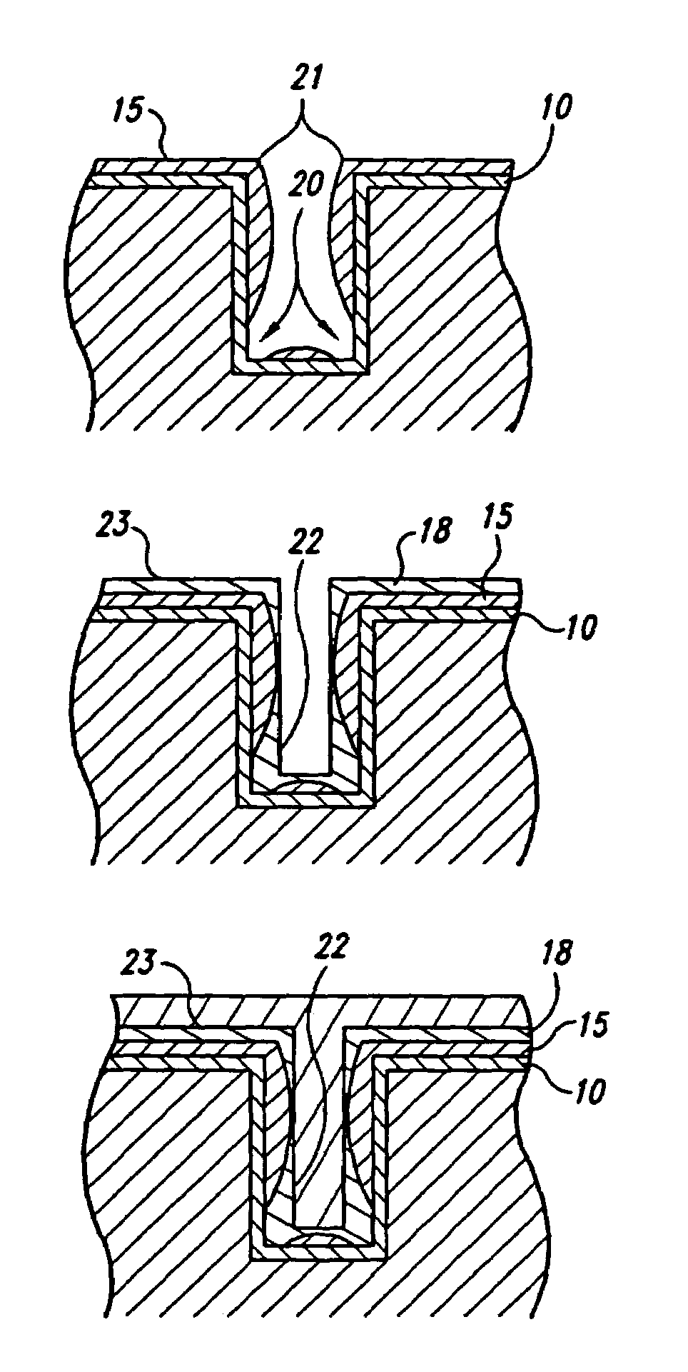
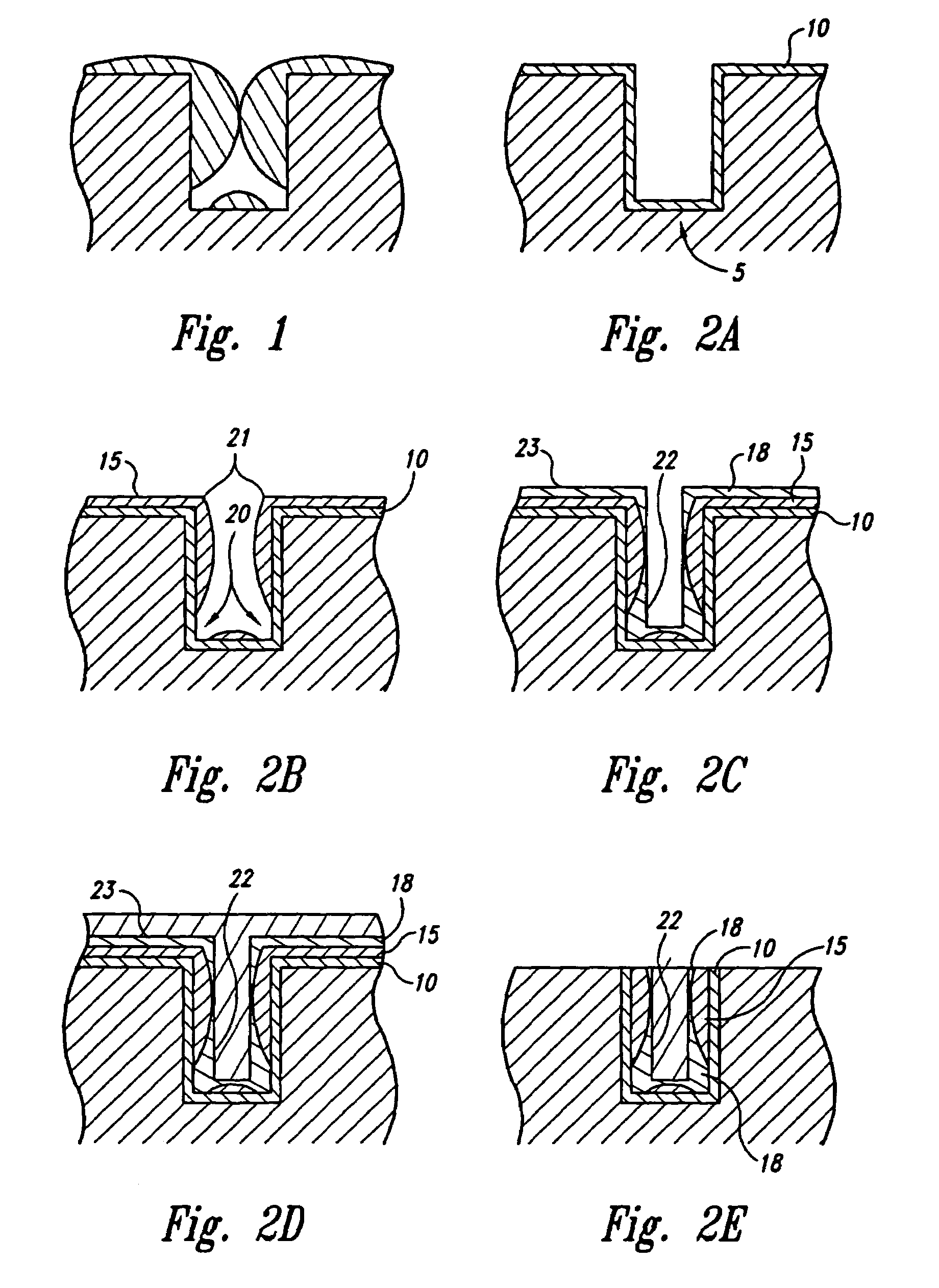
[0030]The resulting metal layer provides an excellent conformal copper coating that fills trenches, vias, and other microstructures in the workpiece. When used for seed layer enhancement, the resulting metal seed layer provides an excellent conformal metal coating that allows the microstructures to be filled with a copper layer having good uniformity using electrochemical deposition techniques. Further, metal layers that are electroplated in the disclosed manner exhibit low sheet resistance and are readily annealed at low temperatures.
[0034]In an alternate embodiment, the seed layer may be enhanced by using an electroless plating bath composition, such as an electroless copper sulfuric acid bath.
Problems solved by technology
The first deposition process anchors the ultra-thin metal seed layer to an underlying layer, the ultra-thin metal seed layer having physical characteristics that render it generally unsuitable for bulk electrolytic deposition of a metal onto the metal seed layer.
The first deposition process anchors the ultra-thin metal seed layer to an underlying layer, the ultra-thin metal seed layer having physical characteristics that render it generally unsuitable for bulk electrolytic deposition of a metal onto the metal seed layer.
The first deposition process anchors the ultra-thin metal seed layer to an underlying layer, the ultra-thin metal seed layer having physical characteristics that render it generally unsuitable for bulk electrolytic deposition of a metal onto the metal seed layer.
Method used
Image
Click on the blue label to locate the original text in one second.
Reading with bidirectional positioning of images and text.
Examples
example 1
[0097]Comparison of Acid Copper Plating
[0098]With and Without Seed Layer Enhancement
[0099]Semiconductor wafers 1, 2 and 3 were each coated with a 200 Angstrom PVD copper seed layer. In accordance with the present invention, wafers 1 and 2 had seed layer enhancement from citric acid and EDTA baths, respectively, the compositions of which are set forth below:
[0100]Bath for Wafer 1: 0.1 M Cu SO4+0.2 M Citric acid+0.05 M H3BO3 in D.I. water at pH 9.5, temperature 25° C.
[0101]Bath for Wafer 2: 0.1 M Cu SO4+0.2 M EDTA acid+0.05 H3BO3 in D.I. water at pH 12.5. temperature 25° C.
[0102]Wafer 3 did not have any Seed Layer Enhancement.
[0103]The three wafers were then plated with a 1.5 micron copper layer from an acid copper bath under identical conditions. The following Table compares the uniformities, as deduced from sheet resistance measurements, of the three wafers after the deposition of a copper layer having a nominal thickness of 1.5 microns.
[0104]
TABLE 1Non-uniformityEnhancementCurrentS...
PUM
Property
Measurement
Unit
thickness
aaaaa
aaaaa
thickness
aaaaa
aaaaa
diameter
aaaaa
aaaaa
Abstract
A process for metallization of a workpiece, such as a semiconductor workpiece. In an embodiment, an alkaline electrolytic copper bath is used to electroplate copper onto a seed layer, electroplate copper directly onto a barrier layer material, or enhance an ultra-thin copper seed layer which has been deposited on the barrier layer using a deposition process such as PVD. The resulting copper layer provides an excellent conformal copper coating that fills trenches, vias, and other microstructures in the workpiece. When used for seed layer enhancement, the resulting copper seed layer provide an excellent conformal copper coating that allows the microstructures to be filled with a copper layer having good uniformity using electrochemical deposition techniques. Further, copper layers that are electroplated in the disclosed manner exhibit low sheet resistance and are readily annealed at low temperatures.
Description
CROSS-REFERENCE TO RELATED APPLICATIONS[0001]The present application is a divisional of U.S. patent application Ser. No. 09 / 732,513, filed Dec. 7, 2000, now U.S. Pat. No. 6,565,729, which is a continuation-in-part of U.S. patent application Ser. No. 09 / 387,099, filed Aug. 31, 1999, now U.S. Pat. No. 6,277,263, which is a continuation of International Patent Application No. PCT / US99 / 06306, filed Mar. 22, 1999, designating the United States, which is a continuation-in-part of U.S. patent application Ser. No. 09 / 045,245, filed Mar. 20, 1998, now U.S. Pat. No. 6,197,181, and claiming the benefit of U.S. Provisional Patent Application No. 60 / 085,675, filed May 15, 1998; and U.S. patent application Ser. No. 09 / 732,513 is also a continuation-in-part of International Patent Application No. PCT / US00 / 10120, filed Apr. 13, 2000, designating the United States and claiming the benefit of U.S. Provisional Patent Application Nos. 60 / 182,160, filed Feb. 14, 2000, 60 / 143,769, filed Jul. 12, 1999, an...
Claims
Application Information
Patent Timeline
Application Date:The date an application was filed.
Publication Date:The date a patent or application was officially published.
First Publication Date:The earliest publication date of a patent with the same application number.
Issue Date:Publication date of the patent grant document.
PCT Entry Date:The Entry date of PCT National Phase.
Estimated Expiry Date:The statutory expiry date of a patent right according to the Patent Law, and it is the longest term of protection that the patent right can achieve without the termination of the patent right due to other reasons(Term extension factor has been taken into account ).
Invalid Date:Actual expiry date is based on effective date or publication date of legal transaction data of invalid patent.

