FinFET transistor and circuit

a transistor and finfet technology, applied in the field of finfet transistors and circuits, can solve the problem that there is no current method for doing this for circuits made up of finfets

Active Publication Date: 2006-10-03
GLOBALFOUNDRIES US INC
View PDF16 Cites 175 Cited by
  • Summary
  • Abstract
  • Description
  • Claims
  • Application Information

AI Technical Summary

Problems solved by technology

At the high performance levels utilizing sub-65 nm dimensions, very fine tuning the drive strengths of transistors in integrated circuits becomes critical, however, no method presently exists for doing this for circuits made up of FinFETs because of the quantized nature of their structures.

Method used


Image

  • FinFET transistor and circuit
  • FinFET transistor and circuit
  • FinFET transistor and circuit

Examples


first embodiment

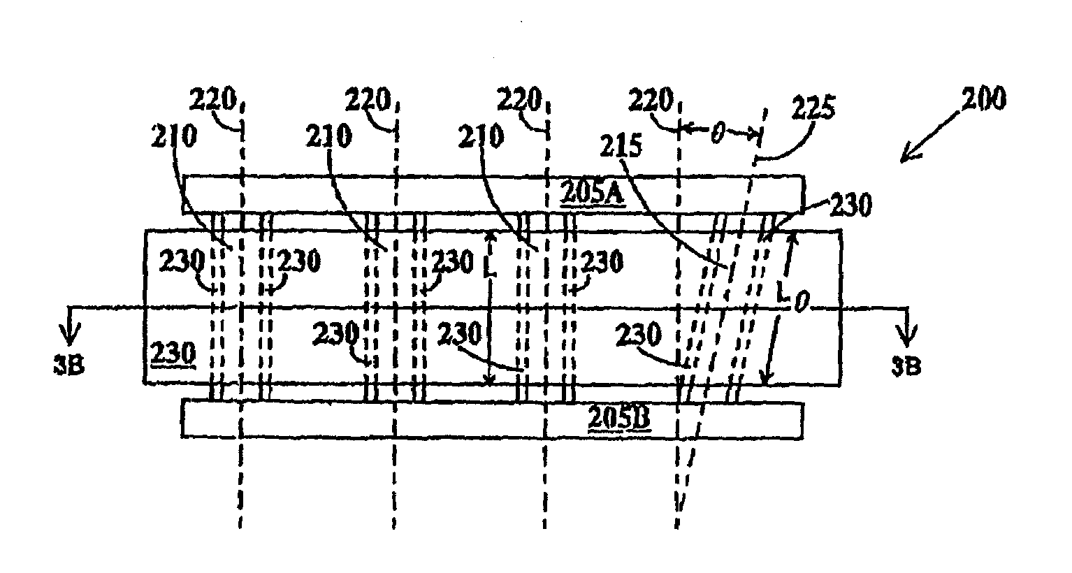
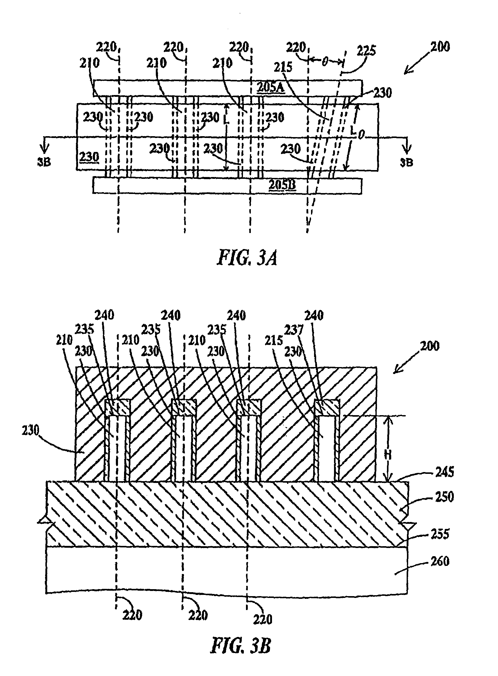
[0028]FIG. 3A is a top view and FIG. 3B is a side view through line 3B—3B of FIG. 3A of a FinFET transistor according to the present invention. In FIG. 3A, FinFET 200 includes parallel source / drains 205A and 205B in physical and electrical contact with opposite ends of single-crystal perpendicular fins 210 and an angled single-crystal fin 215. Perpendicular fins 210 are longitudinally aligned with a plane 220, while angled fin 215 is longitudinally aligned with a plane 225, which is offset (by rotation along a axis common to both planes 210 and 225 as illustrated in FIG. 1 and described supra) from crystal plane 220 by an angle θ. The angle θ also represents a rotation from a higher inversion carrier mobility direction to a lower major carrier mobility direction. Fins 210 are perpendicular to source / drains 205A and 205B. A common gate 230 is formed over perpendicular fins 210 and angled fin 215 and is electrically isolated from the fins by gate dielectric 235 formed on opposite side...

second embodiment

[0046]Before describing the present invention the terms double-gate and split-gate need to be defined. A double-gate transistor is defined as a transistor having two dependent gates, in the case of a FinFET, the gates are located on opposing sidewalls of the fin and electrically connected. They may be integral to one another as well, as is illustrated in FIGS. 4A and 4B. A split-gate transistor is defined as a transistor having two independent gates, in the case of a FinFET, the gates are located on opposing sidewalls of the fin and are electrically isolated from one another.

[0047]FIG. 4A is a top view and FIG. 4B is a side view through line 4B—4B of FIG. 4A of a FinFET transistor according to a second embodiment of the present invention. In FIG. 4A, FinFET 300 includes parallel source / drains 305A and 305B in physical and electrical contact with opposite ends of single-crystal double-gate fins 310 and a single-crystal split-gate fin 315. Double-gate fins 310 and split-gate fin 315 a...


PUM


Abstract

A drive strength tunable FinFET, a method of drive strength tuning a FinFET, a drive strength ratio tuned FinFET circuit and a method of drive strength tuning a FinFET, wherein the FinFET has either at least one perpendicular and at least one angled fin or has at least one double-gated fin and one split-gated fin.

Description

BACKGROUND OF INVENTION[0001]1. Field of the Invention[0002]The present invention relates to the field of FinFET (fin field effect transistors); more specifically, it relates to FinFETs with tuned drive strength, methods tuning the drive strength of FinFETs and circuits utilizing FinFETs with tuned drive strengths.[0003]2. Background of the Invention[0004]Integrated circuit technology and complementary metal-oxide-silicon (CMOS) technology is ever pushed in the direction of higher performance and hence smaller transistor dimensions. Below about 65 nm FinFET technology is emerging as the technology to carry forward the pursuit of high performance circuits. At the high performance levels utilizing sub-65 nm dimensions, very fine tuning the drive strengths of transistors in integrated circuits becomes critical, however, no method presently exists for doing this for circuits made up of FinFETs because of the quantized nature of their structures. Thus, there is a need for fine tunable dr...

Claims


Application Information

Patent Timeline
Patent Type & Authority Patents(United States)
IPC IPC(8): H01L27/10H01L27/08H01L21/335H01L21/336H01L21/8234H01L27/088H01L27/092H01L29/04H01L29/772H01L29/786
CPCH01L29/045H01L29/66795H01L29/785
Inventor BERNSTEIN, KERRYNOWAK, EDWARD J.RAINEY, BETHANN
Owner GLOBALFOUNDRIES US INC
Why Eureka
Try Eureka