Method and apparatus for performing density-biased buffer insertion in an integrated circuit design

a technology of integrated circuit design and buffer, which is applied in the direction of computer aided design, program control, instruments, etc., can solve the problems of increasing the number of buffers required, reducing the delay, and increasing the difficulty of managing the density of the integrated circuit design, so as to minimize the impact of performan

Inactive Publication Date: 2006-11-14
GLOBALFOUNDRIES INC
View PDF12 Cites 10 Cited by
  • Summary
  • Abstract
  • Description
  • Claims
  • Application Information

AI Technical Summary

Problems solved by technology

As gate delays decrease with increasing chip dimensions, however, the number of buffers required quickly rises.
In addition to timing issues, managing the density of an integrated circuit design is becoming more problematic.
If the logic is completely spread out, the design is routable but the performance suffers significantly.
A packed design is unsuitable for later design changes, such as the insertion of additional logic, such as a synthesized clock tree, since there is no room for the new logic.
One problem with the van Ginneken approach to buffer insertion is that buffers are inserted at uniformly placed points along a net.

Method used


Image

  • Method and apparatus for performing density-biased buffer insertion in an integrated circuit design
  • Method and apparatus for performing density-biased buffer insertion in an integrated circuit design
  • Method and apparatus for performing density-biased buffer insertion in an integrated circuit design

Examples


Embodiment Construction

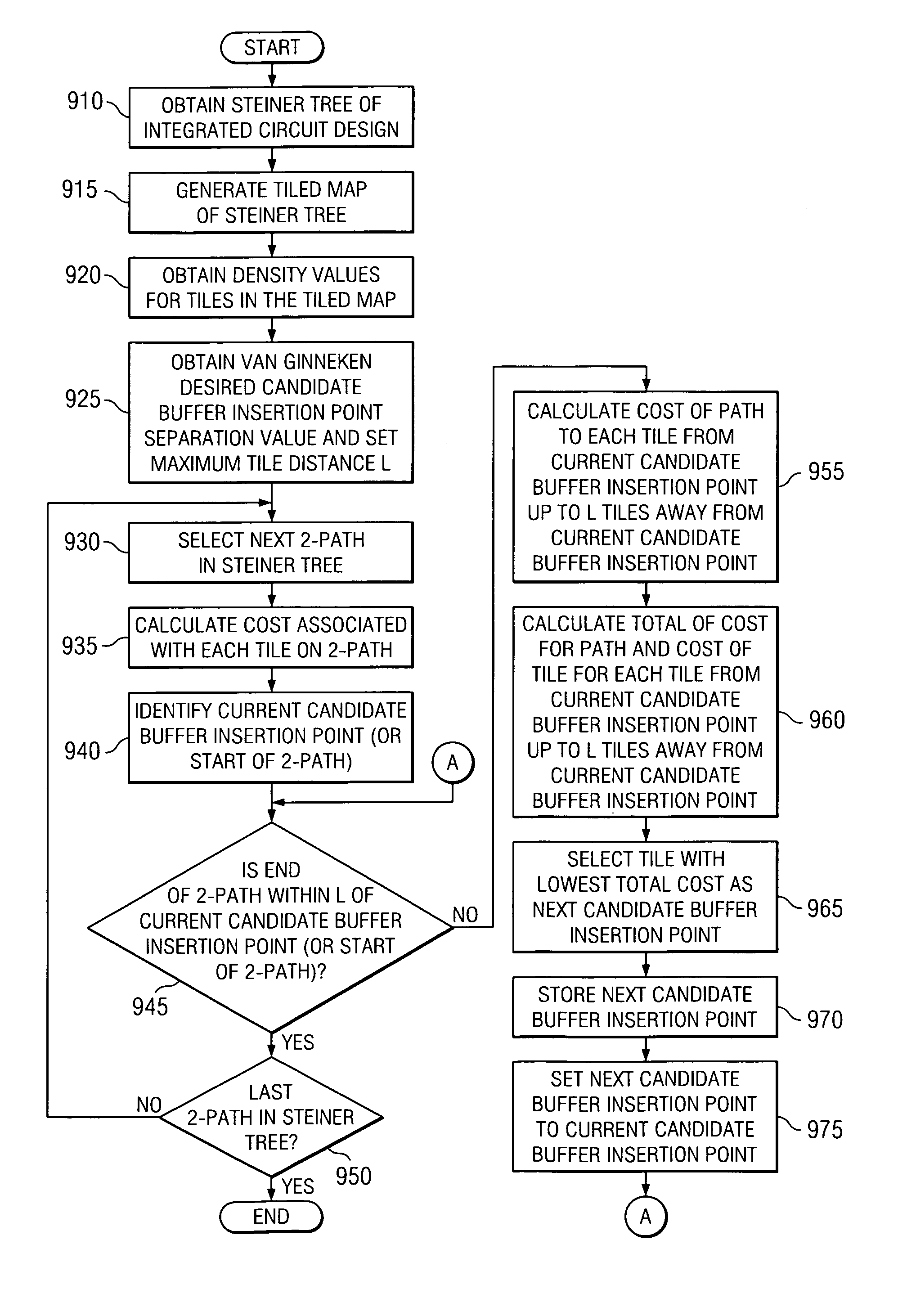
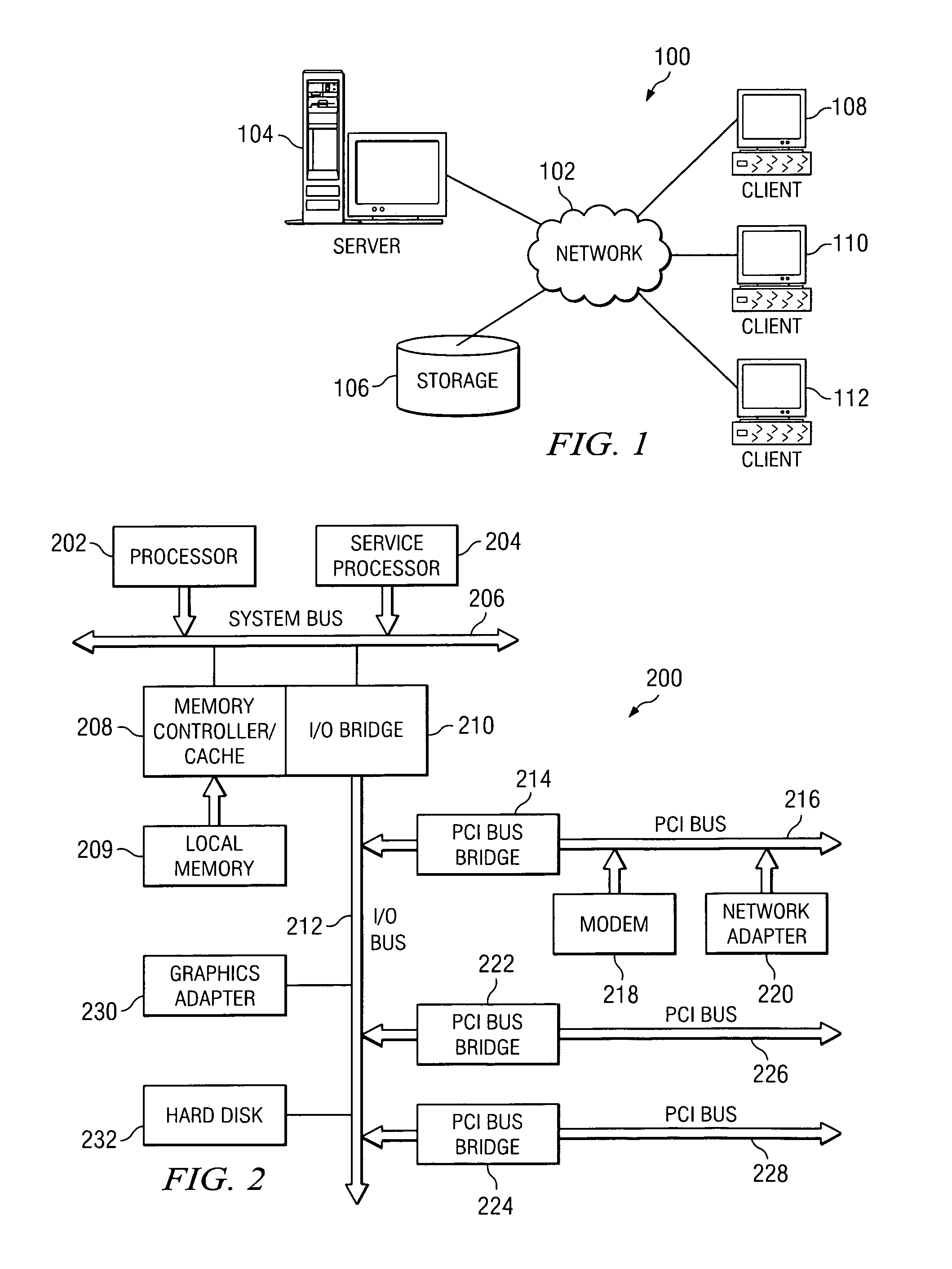
[0027]The present invention provides a method, apparatus and computer program product for performing density-biased buffer insertion in an integrated circuit design. As such, the present invention is preferably implemented in a data processing device. The data processing device may be a stand-alone computing device or may be a distributed data processing system in which multiple computing devices are utilized to perform various aspects of the present invention. Therefore, the following FIGS. 1 and 2 are provided as exemplary diagrams of data processing environments in which the present invention may be implemented. It should be appreciated that FIGS. 1 and 2 are only exemplary and are not intended to assert or imply any limitation with regard to the environments in which the present invention may be implemented. Many modifications to the depicted environments may be made without departing from the spirit and scope of the present invention.

[0028]With reference now to the figures, FIG...


PUM


Abstract

A method, apparatus, and computer program product for performing density biased buffer insertion in an integrated circuit design are provided. A tiled Steiner tree topology map is used in which density values are associated with each tile in the map. A directed acyclic graph (DAG) is created over an initial set of potential candidate points. A subset of the candidate points is selected by associating costs with each tile, and with each path or edge, to each tile. The total costs associated with placement of a buffer at a position within each tile are calculated. The lowest cost tile is then selected as a candidate position for buffer insertion. This process is then repeated to obtain an asymmetrically distributed set of candidate buffer insertion points between a source and a sink.

Description

BACKGROUND OF THE INVENTION[0001]1. Technical Field[0002]The present invention is directed to an improved method and apparatus for performing buffer insertion into an integrated circuit design. More specifically, the present invention is directed to a buffer insertion technique for efficiently locating candidate buffer insertion locations and managing logic design density within an integrated circuit, wherein the candidate buffer insertion locations are biased based on the relative density of one candidate location to other candidate locations.[0003]2. Description of Related Art[0004]It is now widely accepted that interconnect performance is becoming increasingly dominant over transistor and logic performance in the deep submicron regime. Buffer insertion is now a fundamental technology used in modern integrated circuit design methodologies. As gate delays decrease with increasing chip dimensions, however, the number of buffers required quickly rises. It is expected that close to 80...

Claims


Application Information

Patent Timeline
Patent Type & Authority Patents(United States)
IPC IPC(8): G06F17/50G06F9/45
CPCG06F17/5077G06F30/394
Inventor ALPERT, CHARLES JAYHRKIC, MILOSQUAY, STEPHEN THOMAS
Owner GLOBALFOUNDRIES INC
Why Eureka
Try Eureka