Vias in porous substrates

a porous substrate and via technology, applied in the field of packaging of microelectronic devices, can solve the problems of increasing the amount of silicon, increasing the cost of each chip, and conventional vias may have reliability challenges

Active Publication Date: 2012-10-25
TESSERA LLC
View PDF8 Cites 11 Cited by
  • Summary
  • Abstract
  • Description
  • Claims
  • Application Information

AI Technical Summary

Benefits of technology

[0019]Further aspects of the invention provide systems that incorporate conductive via structures according to the foregoing aspects of the invention, composite chips according to the foregoing aspects of the invention, or both in conjunction with other electronic devices. For example, the system may be disposed in a single housing, which may be a portable housing. Systems according to preferred embodiments in this aspect of the invention may be more compact than comparable conventional systems.

Problems solved by technology

Such a reduction in the available space on the first face that can be used for active circuitry may increase the amount of silicon required to produce each semiconductor chip, thereby potentially increasing the cost of each chip.
Conventional vias may have reliability challenges because of a non-optimal stress distribution inside of the vias and a mismatch of the coefficient of thermal expansion (CTE) between a semiconductor chip, for example, and the structure to which the chip is bonded.
For example, when conductive vias within a semiconductor chip are insulated by a relatively thin and stiff dielectric material, significant stresses may be present within the vias.
In addition, when the semiconductor chip is bonded to conductive elements of a polymeric substrate, the electrical connections between the chip and the higher CTE structure of the substrate will be under stress due to CTE mismatch.

Method used


Image

  • Vias in porous substrates
  • Vias in porous substrates
  • Vias in porous substrates

Examples


Embodiment Construction

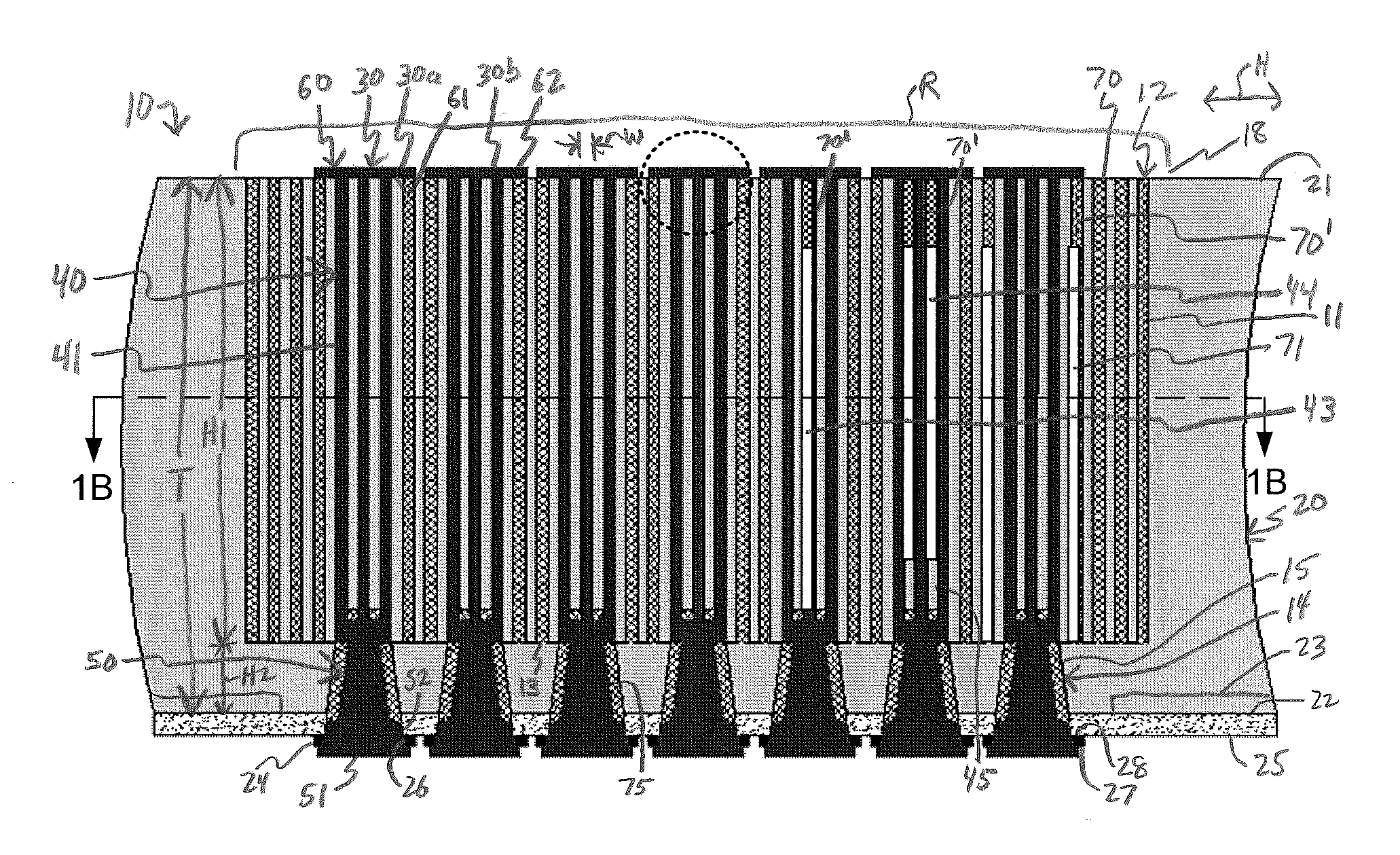
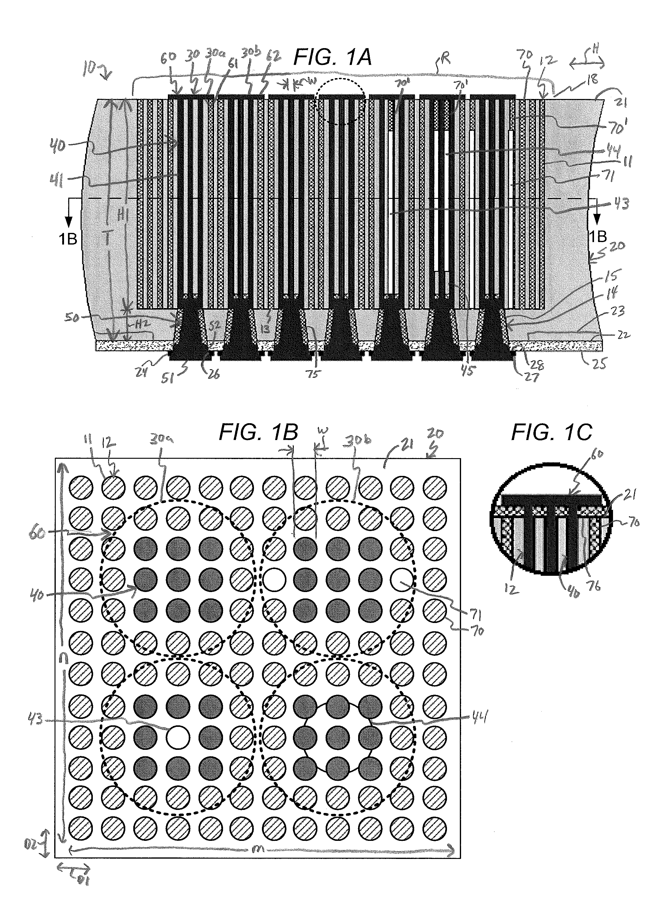
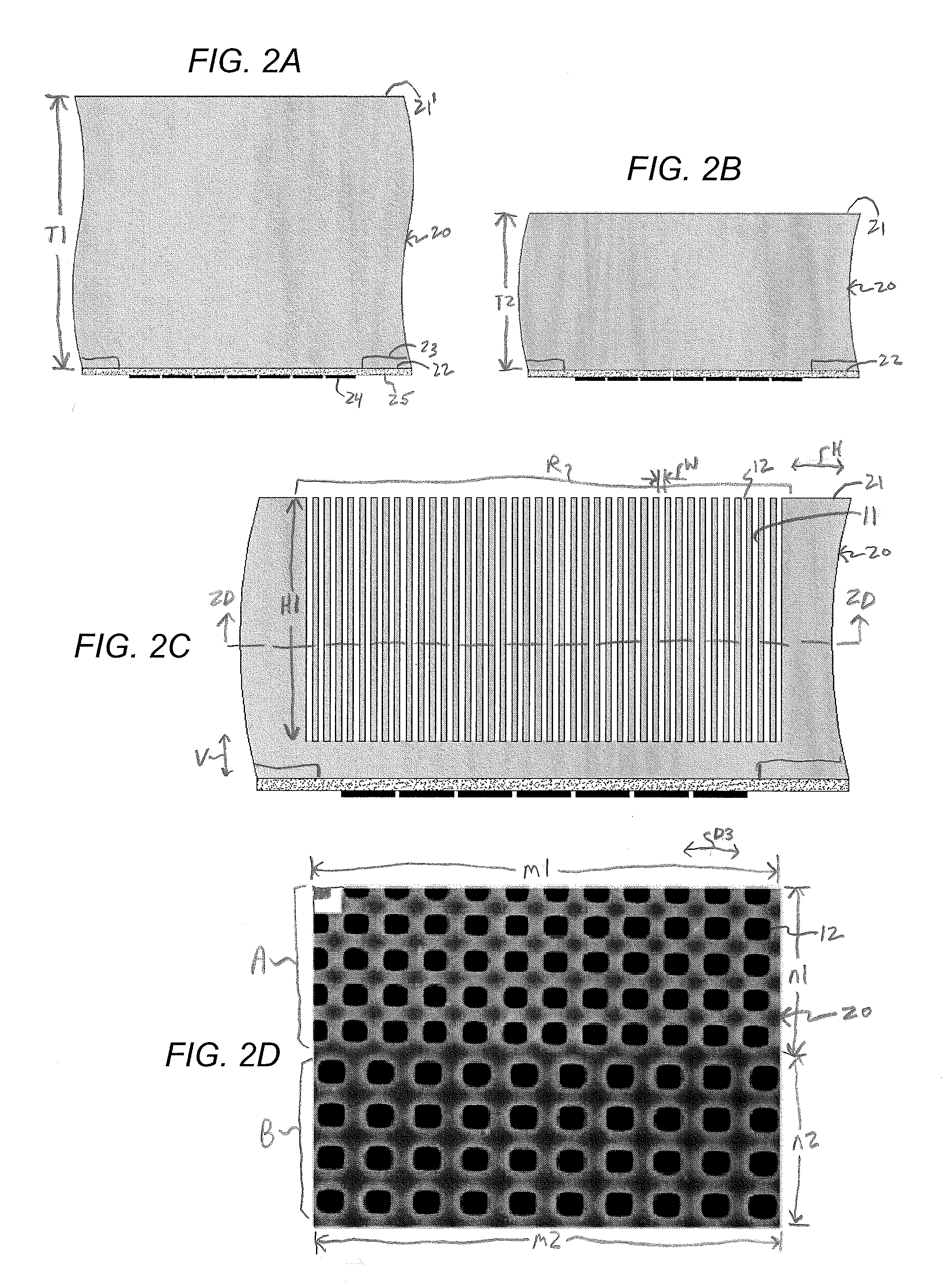
[0046]As illustrated in FIGS. 1A and 1B, a microelectronic unit 10 can include a silicon substrate 20 having a rear surface or first surface 21 and a front surface or second surface 22 remote therefrom and a plurality of through-silicon vias 30 (“TSVs”) extending therethrough between the front and rear surfaces.

[0047]In some embodiments, the microelectronic unit 10 may be a semiconductor chip, a wafer, or the like. The substrate 20 preferably has a coefficient of thermal expansion (“CTE”) less than 8*10−6 / ° C. (or ppm / ° C.). In a particular embodiment, the substrate 20 can have a CTE less than 7*10−6 / ° C. The substrate 20 may consist essentially of an inorganic material such as silicon. In embodiments wherein the substrate 20 is made of a semiconductor, such as silicon, a plurality of active semiconductor devices (e.g., transistors, diodes, etc.) can be disposed in an active semiconductor region 23 thereof located at and / or below the front surface 22. The thickness of the substrate ...


PUM


Abstract

A microelectronic unit can include a substrate having front and rear surfaces and active semiconductor devices therein, the substrate having a plurality of openings arranged in a symmetric or asymmetric distribution across an area of the rear surface, first and second conductive vias connected to first and second pads exposed at the front surface, pluralities of first and second conductive interconnects extending within respective ones of the openings, and first and second conductive contacts exposed for interconnection with an external element. The plurality of first conductive interconnects can be separated from the plurality of second conductive interconnects by at least one of the plurality of openings, the at least one opening at least partially filled with an insulating material. The distribution of the openings can include at least m openings spaced apart in a first direction and n openings spaced apart in a second direction transverse to the first direction.

Description

BACKGROUND OF THE INVENTION[0001]The present invention relates to packaging of microelectronic devices, especially the packaging of semiconductor devices.[0002]Microelectronic elements generally comprise a thin slab of a semiconductor material, such as silicon or gallium arsenide, commonly called a die or a semiconductor chip. Semiconductor chips are commonly provided as individual, prepackaged units. In some unit designs, the semiconductor chip is mounted to a substrate or chip carrier, which is in turn mounted on a circuit panel, such as a printed circuit board.[0003]The active circuitry is fabricated in a first face of the semiconductor chip (e.g., a front surface). To facilitate electrical connection to the active circuitry, the chip is provided with bond pads on the same face. The bond pads are typically placed in a regular array either around the edges of the die or, for many memory devices, in the die center. The bond pads are generally made of a conductive metal, such as cop...

Claims


Application Information

Patent Timeline
Patent Type & Authority Applications(United States)
IPC IPC(8): H01L23/48H01L21/28
CPCH01L21/486H01L21/76898H01L23/147H01L23/15H01L23/481H01L2924/0002H01L23/49827H01L2924/09701H01L2924/00H01L21/76802H01L23/48H01L23/498H01L21/7682H01L21/768H01L21/76837H01L21/76877
Inventor MOHAMMED, ILYASHABA, BELGACEMUZOH, CYPRIANSAVALIA, PIYUSH
Owner TESSERA LLC
Why Eureka
Try Eureka