Large-area imager with direct digital pixel output

Inactive Publication Date: 2006-11-21
XEROX CORP
View PDF9 Cites 27 Cited by
  • Summary
  • Abstract
  • Description
  • Claims
  • Application Information

AI Technical Summary

Benefits of technology

[0013]Based on the aspects and features mentioned above and described herein, the present invention provides an imaging system that scales well with the size of the sensor array. First, the sensor substrate pin (connector) count is independent of the imager size due to the column select circuitry and digital multiplexer that are formed on the sensor substrate. Second, differential current data line signals facilitate recording sensor information for an entire row of pixels without changing the data line voltage. Pixel informat

Problems solved by technology

Several problems are associated with conventional large-area imaging systems.
The large number of required connectors 75 gives rise to increased production costs and other associated problems, such as limited image quality due to data-line noise pickup and/or kTC noise, electromechanical reliability, and production yield.
Therefore, increasing the number of pixel rows and/or columns to increase the imager size or resolution involves increasing the number of connections, which in turn increases production costs and the other assoc

Method used


Image

  • Large-area imager with direct digital pixel output
  • Large-area imager with direct digital pixel output
  • Large-area imager with direct digital pixel output

Examples


Example

DETAILED DESCRIPTION OF THE DRAWINGS

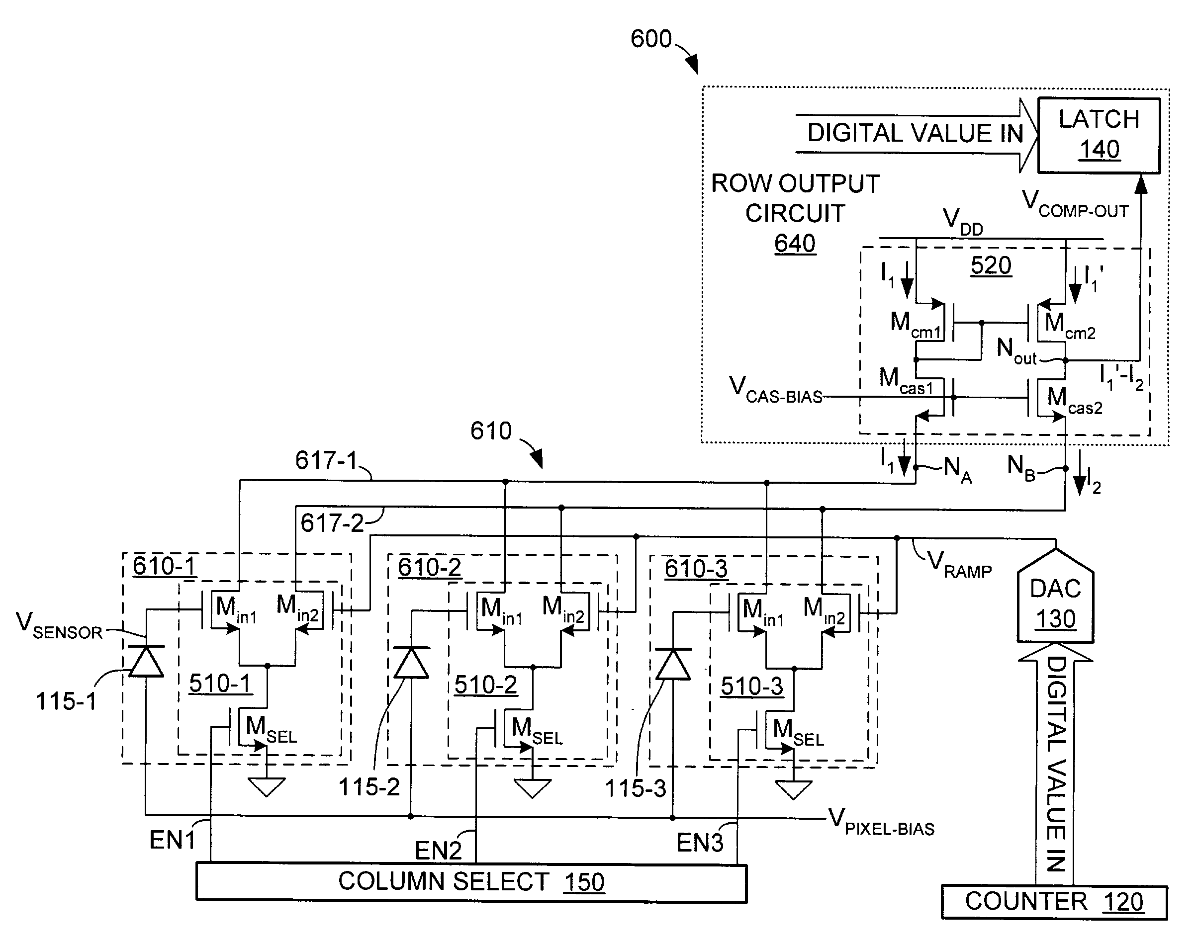
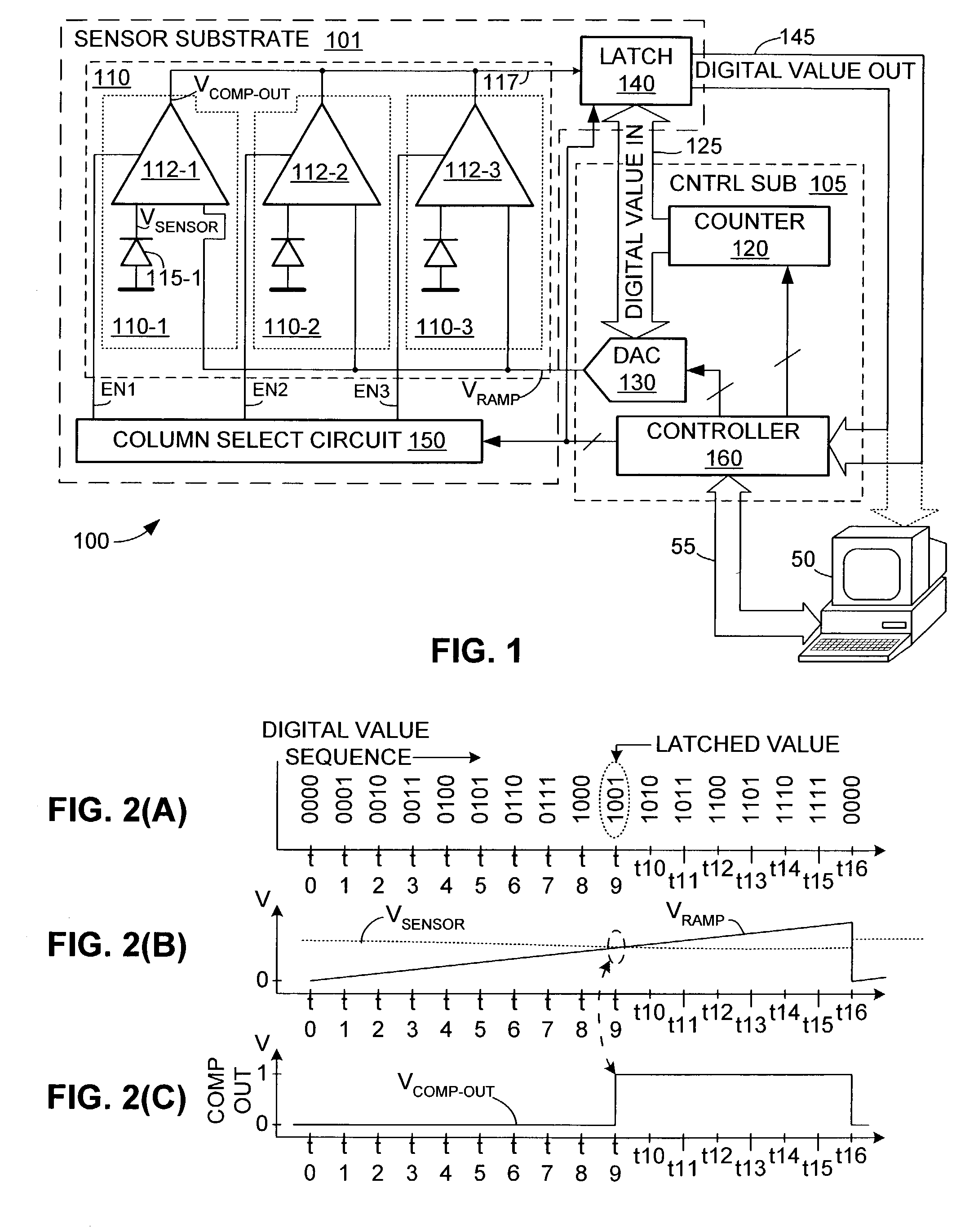
[0026]FIG. 1 is a block diagram showing an imaging system 100 according to a simplified embodiment of the present invention. Imaging system 100 includes an array of pixels 110 arranged in rows and columns (one row including pixels 110-1 through 110-3 is shown), a digital counter 120, a digital-to-analog converter (DAC) 130, at least one edge-triggered latch 140, and a column select circuit 150. In accordance with an aspect of the present invention, pixel array 110, latch 140, and column select circuit 150 are fabricated on a sensor (first) substrate 101, and counter 120 and DAC 130 are separately fabricated on a control / readout substrate (CNTRL SUB) 105, which also includes an optional system control circuit 160. Optional system control circuit 160 generates control signals that are transmitted to the various circuits of imaging system 100, and also coordinates communication between imaging system 100 and an external computer 50 via an external bu...


PUM


Abstract

An imager circuit includes an array of pixels, each pixel including a sensor (photodiode) connected to an input terminal of a comparator. The comparators of each pixel row have output terminals connected to a latch. A counter generates a sequence of digital values that are transmitted to a digital-to-analog converter (DAC) and to the latch of each row. The DAC generates a ramp voltage that is transmitted to a second input terminal of each pixel's comparator. The comparators of a selected pixel column are enabled to generate output signals when the ramp voltage equals each pixel's voltage, causing the associated latches to capture the current digital values. The comparators are formed such that each pixel row shares a cascode mirror circuit that detects differential currents in data line pairs connected to each pixel in that row.

Description

FIELD OF THE INVENTION[0001]This invention relates to imaging devices, and in particular to imaging systems that utilize large-area sensor arrays.BACKGROUND OF THE INVENTION[0002]FIG. 11 is a circuit diagram showing a simplified conventional large-area imaging system (“imager”) 50, which is a well-known device that utilizes a large-area sensor array and associated electronics to capture radiation images (e.g., visible light images, or high-energy X-ray images). Conventional large imaging system 50 includes a large-area sensor substrate 60 (e.g., glass or quartz) having formed thereon pixels 61 that are arranged in rows and columns, and a separate control / readout circuit 70 that is used to drive and read image data from sensor substrate 60 during imager operation. Each pixel 61 typically includes a sensor (radiation detection element) 62 and an access transistor 63, which is typically a thin film transistor (TFT) formed on substrate 60. Each sensor typically includes a photosensitive...

Claims


Application Information

Patent Timeline
IPC IPC(8): H04N3/14H04N5/363H04N5/378
CPCH04N3/155H04N25/767H04N25/772H04N25/75
Inventor LU, JENG PINGVAN SCHUYLENBERGH, KOENRAAD F.
Owner XEROX CORP
Why Eureka
Try Eureka