Image sensing apparatus and method using radiation

a sensing apparatus and radiation technology, applied in the direction of x/gamma/cosmic radiation measurement, radioation controlled devices, instruments, etc., can solve the problems of no sensors that attenuate radiation at all, the layout of sensors is difficult to achieve, and the cost of the entire apparatus is increased

Inactive Publication Date: 2006-12-12
CANON KK
View PDF21 Cites 13 Cited by
  • Summary
  • Abstract
  • Description
  • Claims
  • Application Information

AI Technical Summary

Problems solved by technology

However, when AEC sensors are separately prepared in the radiation image sensing apparatus in which sensors are two-dimensionally arrayed to adjust (AEC-control) an incident radiation dose, the layout of the sensors poses a problem.
If AEC sensors should be laid out without impeding image sensing by image sensing sensors, AEC sensors that attenuate radiation by only a minimum amount must be independently arranged, resulting in an increase in cost of the entire apparatus.
In addition, there are no sensors that do not attenuate radiation at all.
Hence, the quality of a sensed image inevitably degrades.
However, when the number of pixels is, e.g., 2,000×2,000, a high-speed driving circuit is necessary, resulting in an increase in cost of the entire apparatus.
Since high-speed driving is necessary, it is difficult to sufficiently ensure the charge storage time, charge transfer time, and capacitor reset time in the image sensing sensors.
As a result, the quality of a sensed image degrades.
This may complicate the interconnection structure.

Method used


Image

  • Image sensing apparatus and method using radiation
  • Image sensing apparatus and method using radiation
  • Image sensing apparatus and method using radiation

Examples


first embodiment

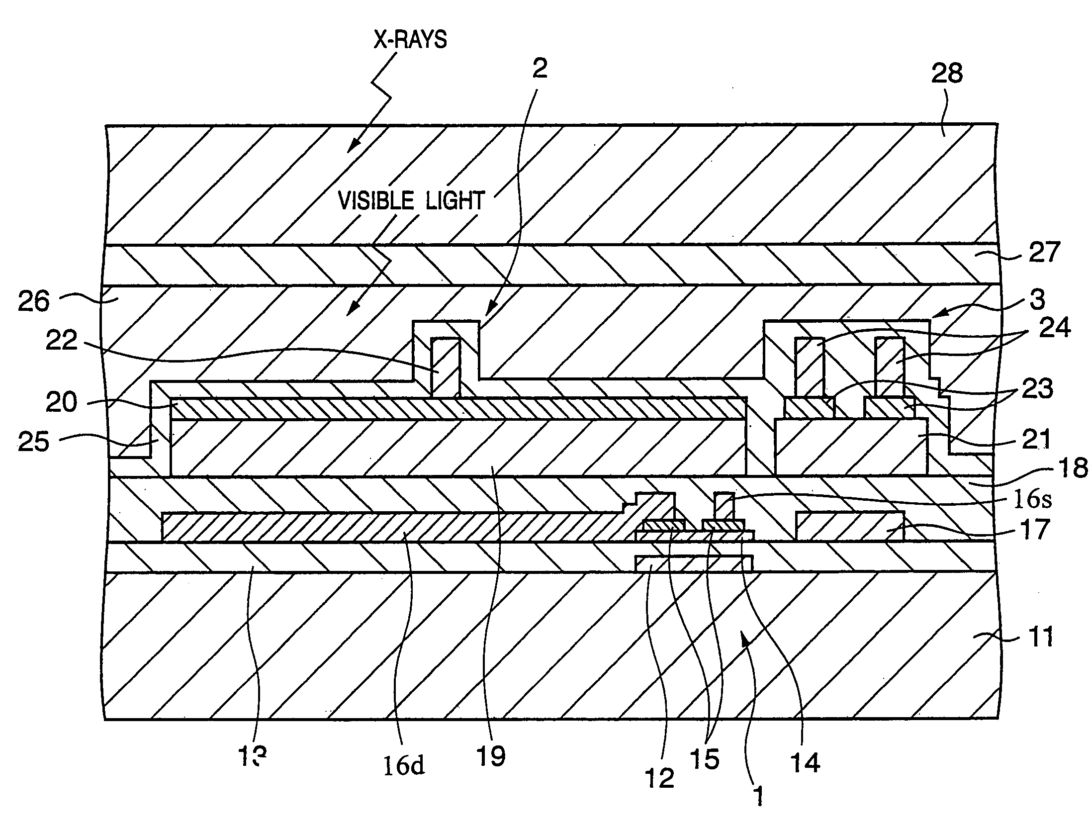
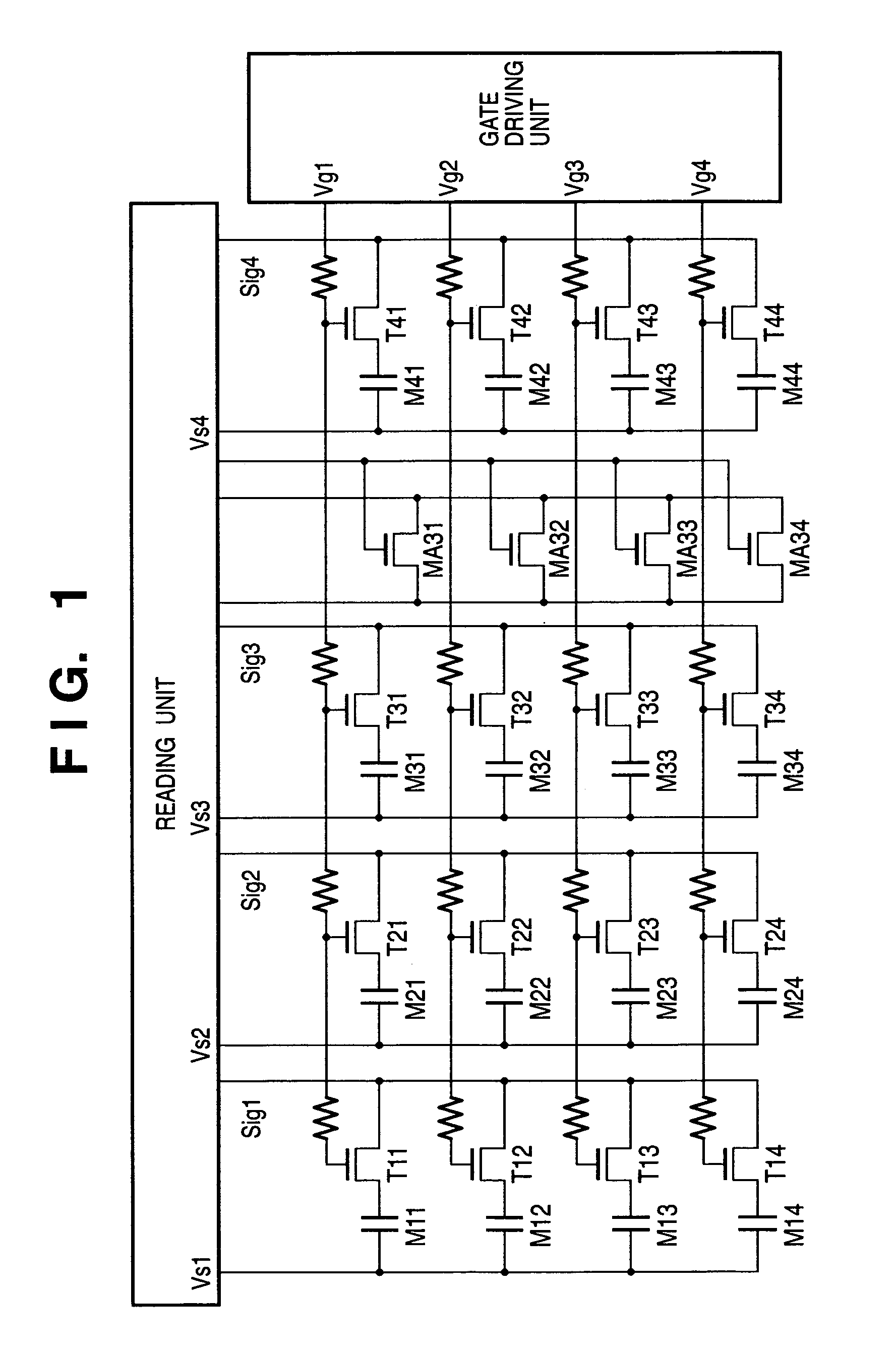
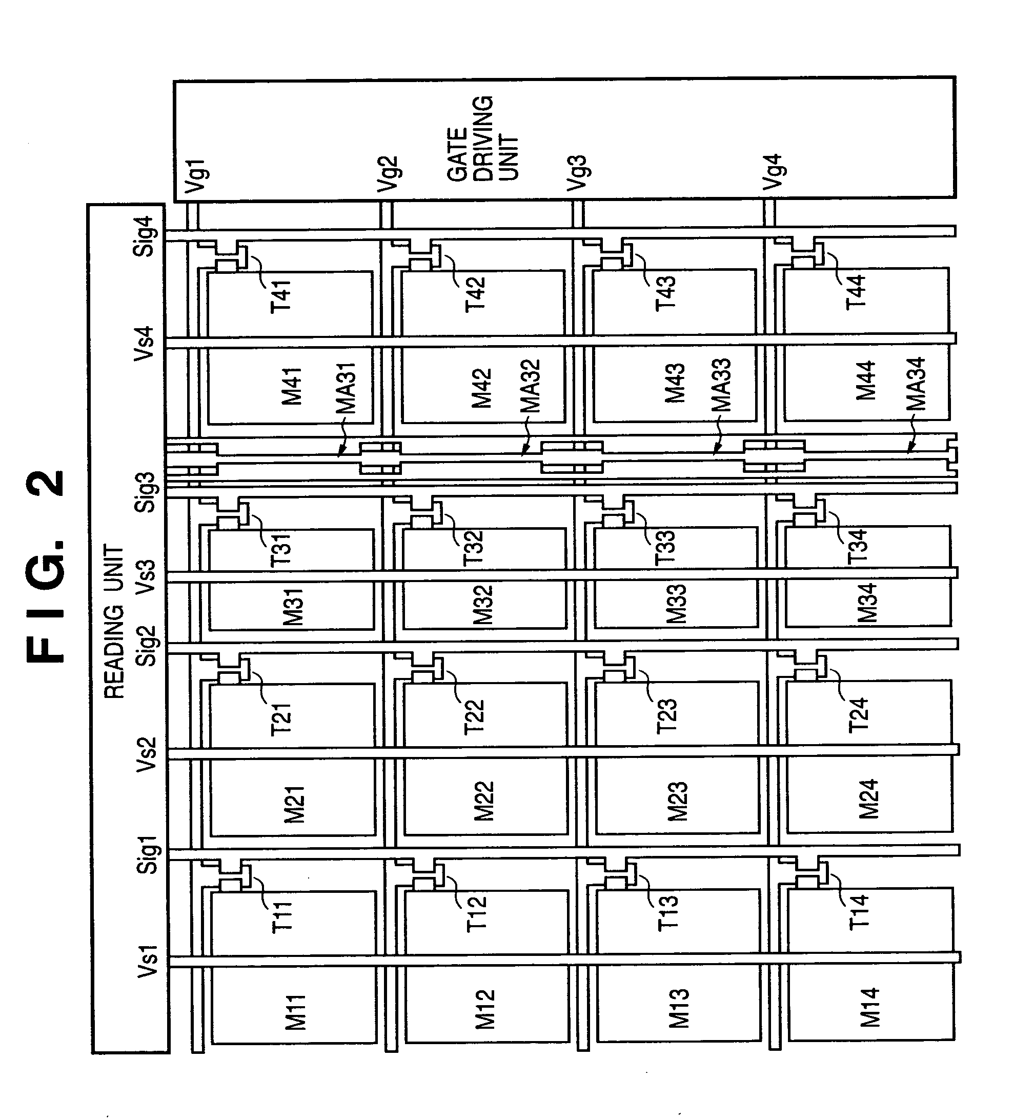
[0079]The first embodiment of the present invention will be described first. FIG. 1 is an equivalent circuit diagram showing the circuit arrangement of a radiation image sensing apparatus according to the first embodiment of the present invention. FIG. 2 is a plan view showing the layout structure of the radiation image sensing apparatus according to the first embodiment. FIG. 3 is a sectional view showing the layer structure of one pixel of the radiation image sensing apparatus according to the first embodiment. FIGS. 1 and 2 show an example in which 4 (rows)×4 (columns) (=a total of 16) pixels are arranged in a pixel area. However, the number of pixels is not limited to this. For example, 2,000×2,000 pixels may be arranged. Semiconductor conversion elements here include an optical conversion element which converts light into charges and a radiation conversion element which directly converts radiation into charges.

[0080]In this embodiment, a combination of a MIS photoelectric conve...

second embodiment

[0102]The second embodiment of the present invention will be described next. FIG. 4 is an equivalent circuit diagram showing the circuit arrangement of a radiation image sensing apparatus according to the second embodiment of the present invention. FIG. 5 is a plan view showing the layout structure of the radiation image sensing apparatus according to the second embodiment. FIG. 6 is a sectional view showing the layer structure of one pixel of the radiation image sensing apparatus according to the second embodiment. FIGS. 4 and 5 show an example in which 4 (rows)×4 (columns) (=a total of 16) pixels are arranged in a pixel area, as in the first embodiment. However, the number of pixels is not limited to this. For example, 2,000×2,000 pixels may be arranged.

[0103]In this embodiment, a combination of a PIN photoelectric conversion element (first semiconductor conversion element) and a read TFT (switch element) or a combination of a PIN photoelectric conversion element (first semiconduc...

third embodiment

[0126]The third embodiment of the present invention will be described next. In this embodiment, a combination of a photoconductive element (first photoconductive element), read TFT (switch element), and image sensing capacitor (capacitive element) or a combination of a photoconductive element (first photoconductive element), read TFT (switch element), image sensing capacitor (capacitive element), and photoconductive sensor (second photoconductive element) for AEC is arranged for each pixel.

[0127]The layer structure of a pixel having a photoconductive sensor will be described here with reference to FIG. 7. FIG. 7 is a sectional view showing the layer structure of one pixel of a radiation image sensing apparatus according to the third embodiment of the present invention. This pixel has an etching-stopper-type read TFT 4, photoconductive element 7, photoconductive sensor 8, and image sensing capacitor 9. The structure of the read TFT 4 is the same as in the second embodiment.

[0128]As t...


PUM


Abstract

This invention is to provide a radiation image sensing apparatus capable of automatically adjusting an incident radiation dose without requiring high-speed driving while suppressing any attenuation of the radiation before detection, and a method of manufacturing the same. To accomplish this, a read TFT (1) is formed on an insulating substrate (11). The semiconductor layer (19) and n+-semiconductor layer (20) of an MIS photoelectric conversion element (2) are formed on a second insulating layer (18) that covers the read TFT (1) to be aligned with source and drain electrodes (16) functioning as lower electrodes. The semiconductor layer (21) of a TFT sensor (3) is formed to be aligned with a gate electrode (17) when viewed from the upper side. The semiconductor layers (19, 21) are formed from the same layer. The upper electrode (22) of the MIS photoelectric conversion element (2) is formed on the n+-semiconductor layer (20). Two ohmic contact layers (23) are formed on the semiconductor layer (21). Source and drain electrodes (24) are formed on the two ohmic contact layers (23), respectively.

Description

FIELD OF THE INVENTION[0001]The present invention relates to a radiation image sensing apparatus suitable for a medical image diagnostic apparatus, a nondestructive inspection apparatus, and an analyzing apparatus using radiation and a method of manufacturing the radiation image sensing apparatus.BACKGROUND OF THE INVENTION[0002]A typical radiation image sensing apparatus that has conventionally been used is an apparatus that combines a photosensor having a MIS-TFT structure constructed by a MIS photoelectric conversion element and a switching TFT and a phosphor to convert radiation into visible light. In this specification, radiation includes not only α-rays, β-rays, and γ-rays but also electromagnetic waves such as visible light and X-rays.[0003]FIG. 9 is an equivalent circuit diagram showing the circuit arrangement of a conventional radiation image sensing apparatus. FIG. 10 is a plan view showing the layout structure in the conventional radiation image sensing apparatus.[0004]As...

Claims


Application Information

Patent Timeline
Patent Type & Authority Patents(United States)
IPC IPC(8): G01T1/24G01T1/02G01T1/29
CPCG01T1/026G01T1/24G01T1/2928
Inventor ISHII, TAKAMASAWATANABE, MINORU
Owner CANON KK
Why Eureka
Try Eureka