Solid-state imaging apparatus

a solid-state imaging and apparatus technology, applied in the scanning details of television systems, picture signal generators, television systems, etc., can solve the problems of reduced sn ratio (signal to noise ratio), increased number of elements within a pixel, and reduced pd area

Inactive Publication Date: 2010-07-22
CANON KK
View PDF22 Cites 132 Cited by
  • Summary
  • Abstract
  • Description
  • Claims
  • Application Information

AI Technical Summary

Problems solved by technology

However, Japanese Patent Application Laid-Open No. 2000-232216 increases the FD capacitor itself by having a common FD, and thus has a problem of a degraded SN ratio (Signal to Noise ratio).
Moreover, Japanese Patent

Method used


Image

  • Solid-state imaging apparatus
  • Solid-state imaging apparatus
  • Solid-state imaging apparatus

Examples


first embodiment

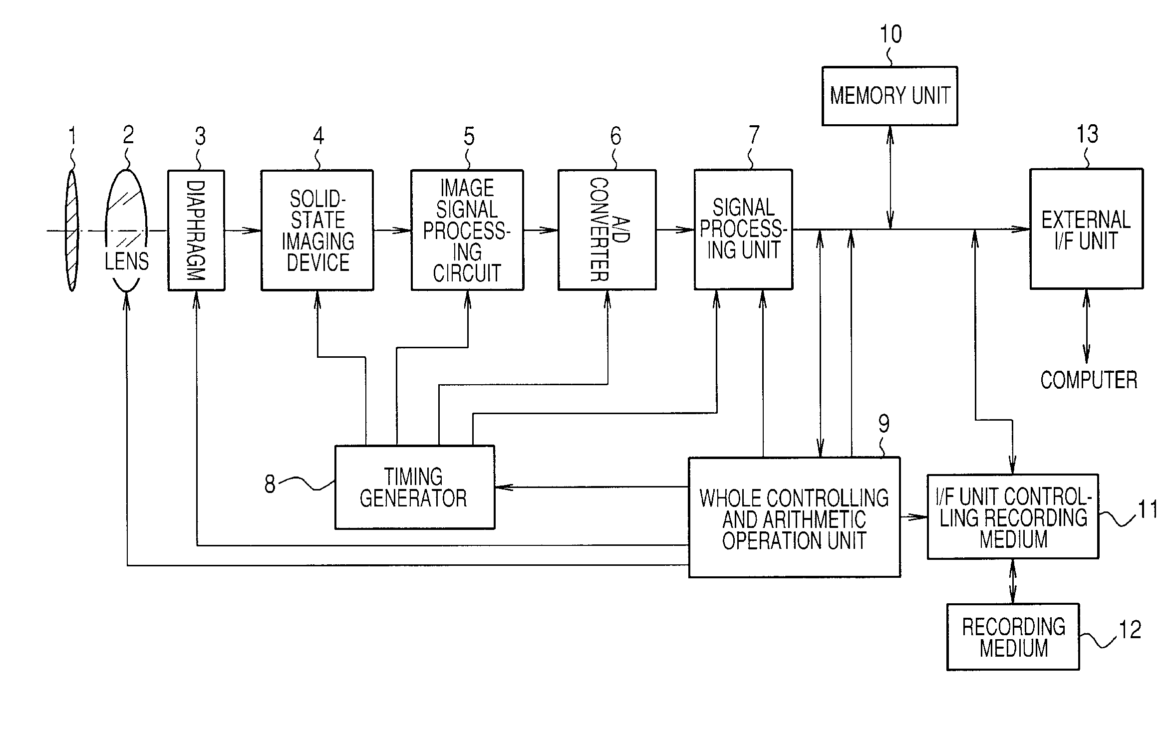
[0030]FIG. 1 illustrates a circuit for two pixels in a solid-state imaging apparatus according to a first embodiment of the present invention. Photodiodes (PDs) 101a and 101b are photoelectric conversion elements for generating an electric charge by photoelectric conversion. Each of transfer transistors 102a and 102b transfers the electric charge generated in each of the photodiodes 101a and 101b to each of floating diffusion (FD) regions 103a and 103b. Source follower (SF) amplifiers (amplifiers) 104a and 104b output voltages which have been electric charge-voltage converted in the FD regions 103a and 103b. Selecting transistors 105a and 105b control outputs of the source follower amplifiers 104a and 104b, and are connected to a vertical signal line 106. Moreover, the vertical signal line 106 is connected to a constant current source 107.

[0031]The FD region 103a is connected to a reset transistor 108, and an FD connecting transistor (connecting unit) 109 is provided between the FD ...

second embodiment

[0060]FIG. 4 illustrates the pixel circuit in the solid-state imaging apparatus according to a second embodiment of the present invention. FIG. 4 is different from FIG. 1 in that a PD 401a is connected to the FD region 103a through a transfer transistor 402a. Similarly, a photodiode 401b is connected to the FD region 103b through a transfer transistor 402b. In other words, this structure includes two pairs of pixel structures having a common FD region and a common SF amplifier for two PDs, and the FD regions 103a and 103b are connected to each other by the FD connecting transistor 109. Read-out timings are basically the same, though the Psel, the Ptx and the like are increased in addition to the timings illustrated in FIG. 3.

[0061]In this case, in a case of a Bayer array color filter, since the PD 101a and the PD 101b become the same color, and the PDs 401a and 401b also become the same color, addition of the same color is enabled.

[0062]Moreover, the present embodiment has shown the...

third embodiment

[0063]FIGS. 5A and 5B illustrate the pixel circuit in the solid-state imaging apparatus according to a third embodiment of the present invention. FIG. 5A is different from FIG. 4 in that FIG. 5A has a structure including three pairs of pixel structures having the common FD region and the common SF amplifier for two PDs, in which FD regions 103a, 103b and 103c are connected to one another by FD connecting transistors 109 and 109b. Moreover, FIG. 5B is different from FIG. 4 in that the common FD region is included for three PDs. The read-out timings are basically the same, though the Psel, the Ptx, the Padd and the like are increased in addition to the timings illustrated in FIG. 3.

[0064]In this case, in the case of the Bayer array color filter, since the PDs 101a, 101b and 101c become the same color, and the PDs 401a, 401b and 401c also become the same color, there is an effect of enabling the addition of the same color. Color centers of different colors are set at regular intervals ...


PUM


Abstract

A solid-state imaging apparatus wherein an FD capacitor value is variable without increasing the number of elements. There is provided a solid-state imaging apparatus including a plurality of photoelectric conversion elements arranged in a horizontal direction and a vertical direction, for generating an electric charge by photoelectric conversion; a plurality of transfer transistors each connected to each of the photoelectric conversion elements, for transferring the electric charge generated by the plurality of photoelectric conversion elements; a plurality of floating diffusion regions for holding the electric charge transferred by the transfer transistors; a plurality of amplifiers each connected to each of the floating diffusion regions, for amplifying a signal based on the electric charge in the plurality of floating diffusion regions; and a connecting unit for connecting and disconnecting between the plurality of floating diffusion regions.

Description

BACKGROUND OF THE INVENTION[0001]1. Field of the Invention[0002]The present invention relates to a solid-state imaging apparatus.[0003]2. Description of the Related Art[0004]As a solid-state imaging apparatus used for an electronic camera or the like, Japanese Patent Application Laid-Open No. 2000-232216 has been disclosed. The solid-state imaging apparatus has two or more sets of photodiodes (PDs) and transfer MOS transistors, performs reading out to a common floating diffusion (FD) region, and performs amplification by a common source follower MOS transistor.[0005]Moreover, Japanese Patent Application Laid-Open No. 2000-165755 has disclosed a unit for providing a solid-state imaging apparatus in which a MOS capacitor is added to an FD so that an FD capacitor is variable, and sensitivity can be changed corresponding to signal electric charges accumulated in a photoelectric conversion section. It is possible to reduce an output signal amplitude when a large amount of electric charge...

Claims


Application Information

Patent Timeline
IPC IPC(8): H04N5/335H04N5/355H04N5/372H04N5/374H04N9/07
CPCH04N5/343H04N5/347H04N5/37457H04N5/335H01L27/14609H01L27/14643H04N25/42H04N25/46H04N25/00H04N25/778
Inventor OKITA, AKIRA
Owner CANON KK
Why Eureka
Try Eureka