
Solid-state imaging device

a solid-state imaging and imaging device technology, applied in the direction of radioation control devices, television system scanning details, television systems, etc., can solve the problems of inability to read out image information with optimal exposure, and the detection range of photoelectric devices is only narrow, so as to achieve a sharp image. stab

Inactive Publication Date: 2000-04-04
NIKON CORP
View PDF14 Cites 130 Cited by
  • Summary
  • Abstract
  • Description
  • Claims
  • Application Information

AI Technical Summary

Benefits of technology

It is an object of the present invention to overcome the problems in the prior art and to provide photoelectric conversion devices and image sensor arrays comprised thereof and image capture apparatus employing such arrays, which allow a sharp image to be stably obtained despite changes in the brightness of the surroundings. This is achieved by automatically adjusting the exposure time in accordance with the environment in which the photoelectric conversion apparatus is placed.
A color filter of a specific color may be installed above the light-receiving surface of the said one of the main electrodes of the reset transistor and / or above the light-receiving surface of the photoelectric conversion element. Also, color filters having different colors may be installed above the light-receiving surfaces of the said one of the main electrodes of the reset transistor and the photoelectric conversion element. Use of such filters allows the advantages mentioned above for embodiments having such filters.

Problems solved by technology

But whenever there is a sudden change during the exposure interval in the amount of incoming light, it becomes impossible to read out image information with optimal exposure.
However, the conventional photoelectric device can detect only a narrow range of spectral components, using a color filter of a specific color.

Method used


Image

  • Solid-state imaging device
  • Solid-state imaging device
  • Solid-state imaging device

Examples


example embodiment 4

Photoelectric Conversion Device Example Embodiment 4

Next, a photoelectric conversion device 150 and a photoelectric conversion apparatus 1500 according to a fourth example embodiment of the invention will be described with reference to FIGS. 18-22. Features corresponding to features of previously described embodiments are given similar reference characters, but with a "5" for the first digit. Where no specific description is given, the corresponding description above applies.

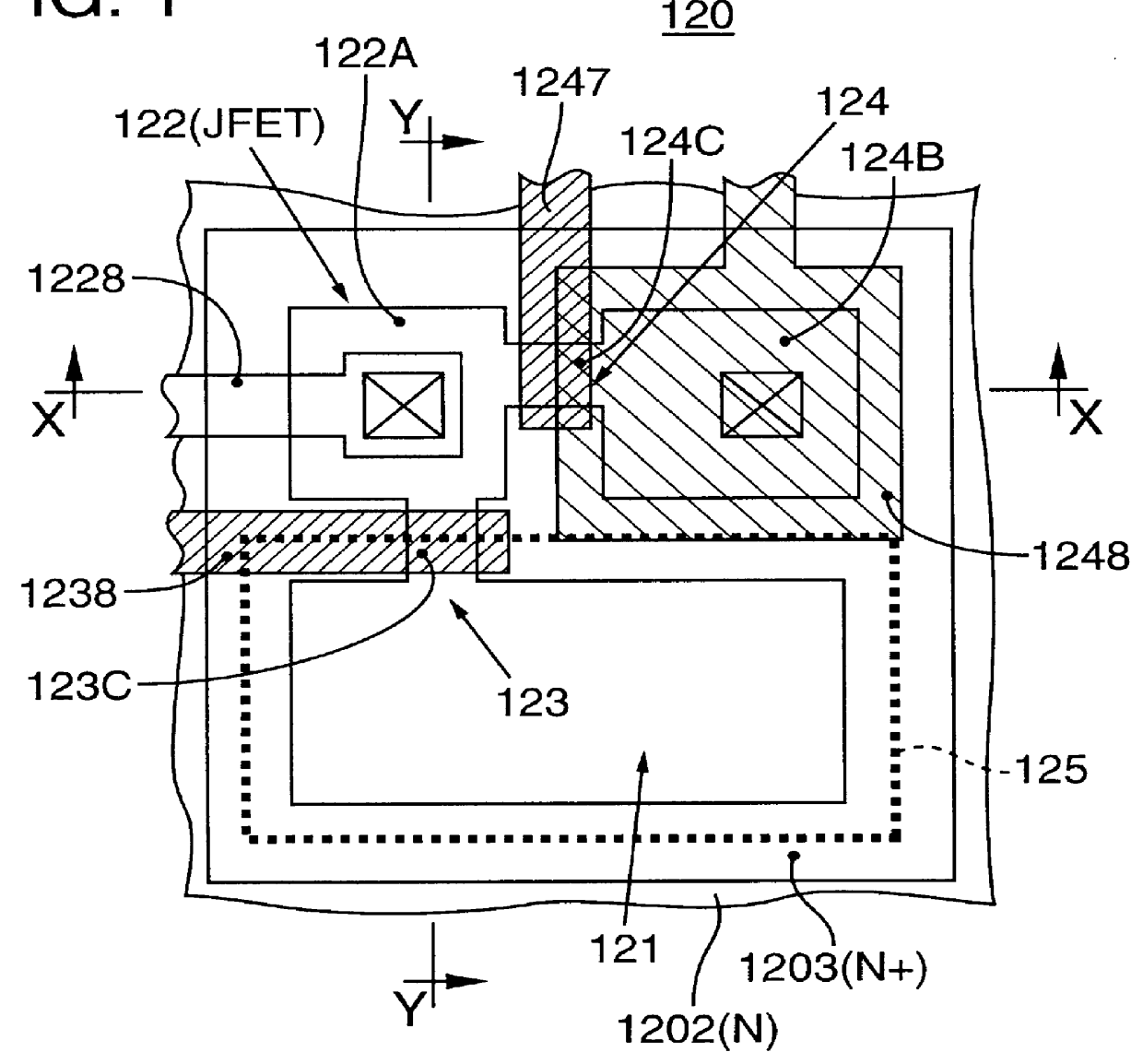
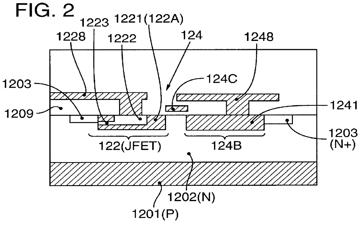
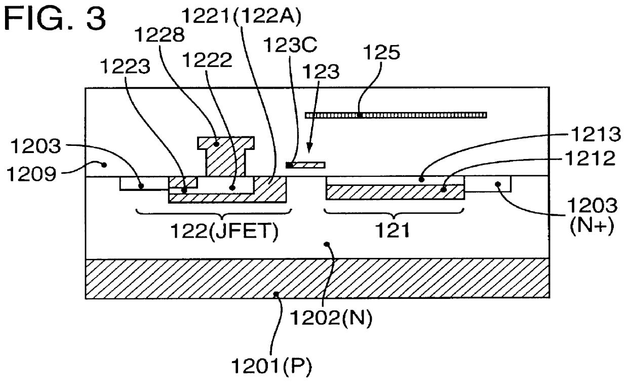
As in the photoelectric conversion device 140 of the third embodiment, the photoelectric conversion device 150 is designed so that light strikes the gate region 152A and the reset drain 154B, as well as the photodiode 151. However, unlike the third embodiment, an electric signal Vout2 corresponding to the signal charge generated by the gate region 152A is output from the source 152B of the JFET 152. An electric signal Vip corresponding to the signal charge generated by the reset drain 154B is output from the out...

first example embodiment

Whereas said first example embodiment is a two-dimensional fixed-image image sensor array, this example embodiment is a one-dimensional fixed-image image sensor array.

This example embodiment comprises a single row of pixels including first pixels, along with related peripheral circuitry.

This embodiment yields the same advantages as the first example embodiment.

Moreover, the modifications previously described for the first example embodiment may be applied similarly to this embodiment as well.

Microlenses Example Embodiments

The image sensor arrays of the present invention can benefit from the use of on-chip microlenses to increase the light-sensitivity and the effective aperture ratio of the arrays. The microlenses of the present invention are specially configured to cooperate with one or more pixels having two photosensitive elements.

example embodiment 1

Microlenses Example Embodiment 1

FIG. 43 shows an example embodiment of a microlens arrangement for use in the context of the present invention. FIG. 43(a) is a plan view and FIG. 43(b) is a cross-sectional view taken along the line A-A' in FIG. 43(a).

In this example embodiment, a single pixel 702A has both a first photoelectric conversion element, such as a photodiode, positioned below an aperture 701, and a second photoelectric conversion element positioned below an aperture 702. The second photoelectric conversion element at aperture 702 is positioned near the center of the fixed-image image sensor array. The pixel 702A is surrounded by conventional single pixels 701A without second photoelectric conversion elements. FIG. 43 represents an enlargement of a single pixel 702A and the surrounding single pixels 701A that form a portion of a larger array of pixels.

In FIG. 43, 701 is the aperture over the first photoelectric conversion element, and 702 is the aperture over the second pho...


PUM


Abstract

A photoelectric conversion device suitable for use as an element of a photodetector array includes a photodiode for generating a first signal charge in response to incident light, an output unit including a JFET, and at least one transistor having an electrode that generates a second signal charge in response to incident light. The first and second signal charges may be output separately or combined. The second signal charge, or the first and second signal charges combined, may be monitored during an exposure time to determine the desired end of the exposure. An image sensor array may have one or more pixels with such light monitoring capability. The output signal for monitoring the light may be output over a reset drain interconnection, directly from the monitoring pixel or through other pixels via inter-pixel MOSFETS. Exposure time may be controlled, by timing a shutter or a strobe or the like, based on the monitored accumulation of signal charge during exposure. Microlenses may be provided on-chip to increase the effective aperture ratio of the array. The microlenses are designed to avoid interfering with the incident light used for monitoring. Resulting pixel-to-pixel variations in effective aperture ratio, if any, may be electronically compensated.

Description

The present invention relates to solid-state imaging devices and photoelectric conversion devices used therein, particularly to image capturing apparatus and image sensor arrays useful in such apparatus for capturing fixed images as in digital photography and the like.Photoelectric conversion devices using photodiodes as photoelectric conversion elements for generating signal charges corresponding to incident light are known in the art. An example of such a photoelectric conversion device is disclosed in, for example, Japanese Laid-Open Patent Application No. 8-293591, which is the subject of U.S. patent application Ser. No. 08 / 606,995, assigned to the assignee of the present application.FIGS. 49, 50, and 51 of the present application show the structure of a photoelectric conversion device as disclosed in Japanese Laid-Open Patent Application No. 8-293591. FIG. 49 is a plan view of a photoelectric conversion device 110, FIG. 50 is a cross-sectional view taken along the line X--X sho...

Claims


Application Information

Patent Timeline
Patent Type & Authority Patents(United States)
IPC IPC(8): H01L27/146H04N3/15H04N5/235H01L27/148H04N5/353H04N5/369
CPCH01L27/14609H01L27/14679H04N5/3745H04N5/353H04N5/2351H04N23/71H04N25/77H04N25/53
Inventor ISHIDA, TOMOHISAOHKOUCHI, NAOKISUZUKI, SATOSHIJUEN, MASAHIROISOGAI, TADAO
Owner NIKON CORP
Learn More