Semiconductor device

a technology of semiconductors and semiconductors, applied in static indicating devices, instruments, material analysis, etc., can solve the problems of low yield, increased power consumption, and inability to easily use optical sensors as photoelectric conversion devices, and achieve low power consumption, small output variation, and high convenience.

Active Publication Date: 2008-07-03
SEMICON ENERGY LAB CO LTD
View PDF52 Cites 131 Cited by
  • Summary
  • Abstract
  • Description
  • Claims
  • Application Information

AI Technical Summary

Benefits of technology

[0082]A wide range of illuminance of several to several tens of thousands of lux can be measured by one optical sensor; thus, a photoelectric conversion device which is highly convenient and has low power consumption can be obtained. Further, since the number of o...

Problems solved by technology

In the case of a conventional optical sensor, when detection of higher illuminance is attempted, output current or output voltage ranges widely, so that the following problems are given: the conventional optical sensor is not easily used as a photoele...

Method used


Image

  • Semiconductor device
  • Semiconductor device
  • Semiconductor device

Examples


embodiment mode 1

[0148]A photoelectric conversion device in this embodiment mode is described with reference to FIGS. 29 to 35. The photoelectric conversion device in this embodiment mode includes a light detection circuit 2900, an amplifier 2903, a comparison circuit 2904, a reference voltage generation circuit 2905, and a control circuit 2906. The light detection circuit 2900 includes an optical sensor 2901 and a current-voltage conversion circuit 2902.

[0149]The light detection circuit 2900 has a function of outputting a voltage signal corresponding to detected illuminance. The optical sensor 2901 has a function of outputting a current signal corresponding to detected illuminance. The current-voltage conversion circuit 2902 includes a current-voltage conversion element and has a function of converting the current signal output from the optical sensor 2901 into a voltage signal. Note that as the optical sensor 2901, a photodiode or a phototransistor can be used. As the current-voltage conversion el...

embodiment mode 2

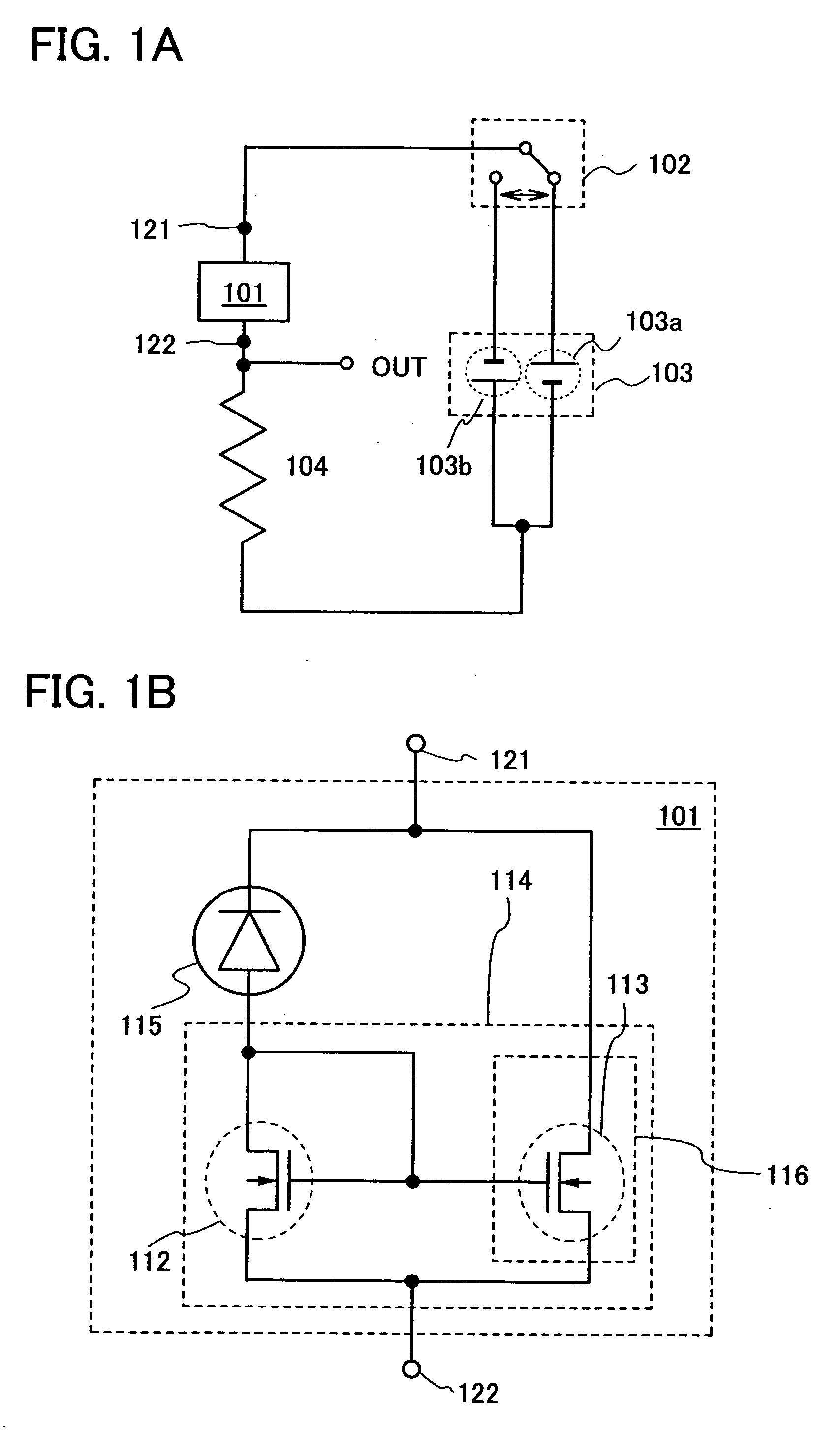
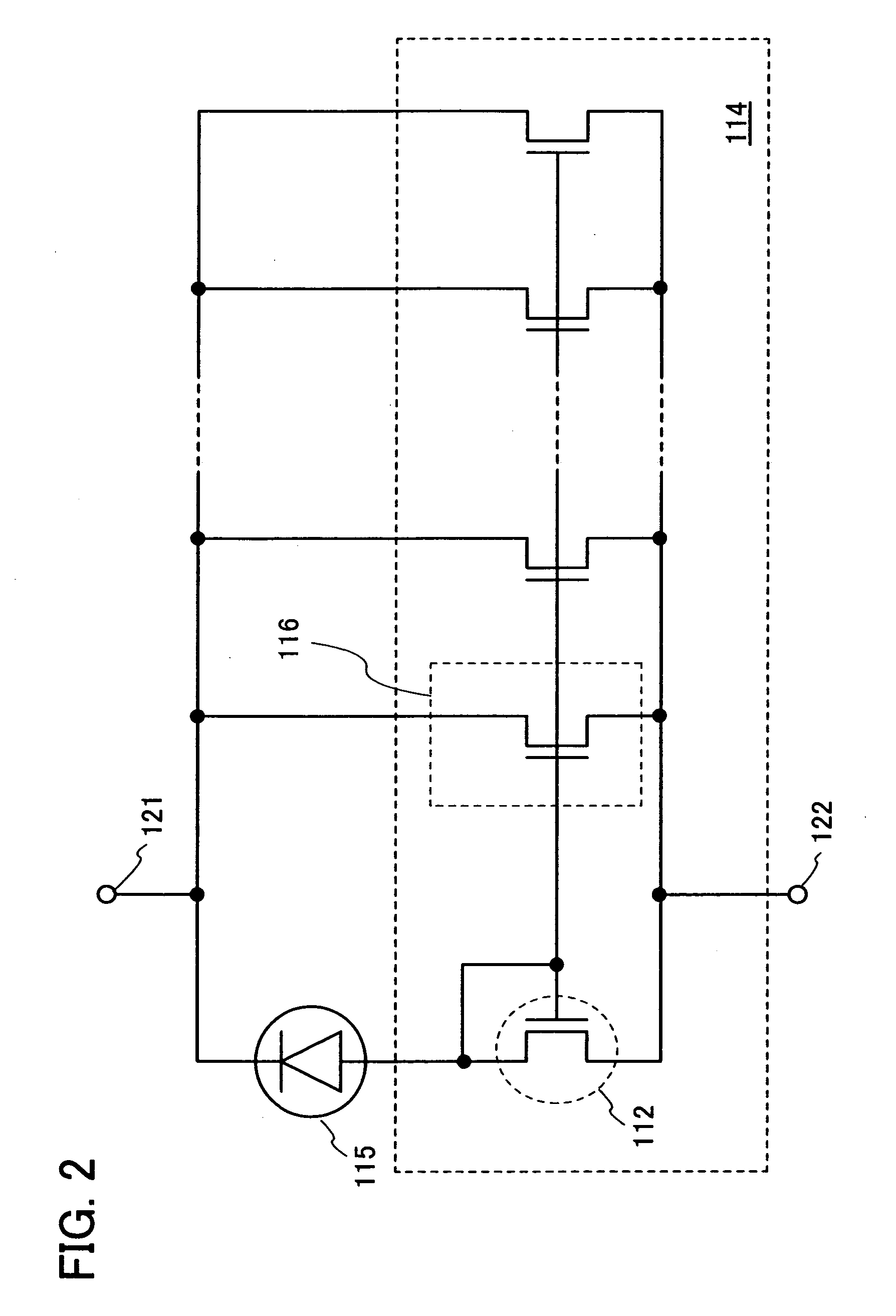
[0226]This embodiment mode is described with reference to FIGS. 1A, 1B, 2, 3A, 3B, 4 to 7, 8A, 8B, 9A to 9D, 10A to 10C, 11A to 11C, 12, and 13. A semiconductor device shown in FIG. 1A includes a photoelectric conversion device 101, a bias switching unit 102, a power supply 103, the terminal OUT, and a resistor 104. The photoelectric conversion device 101 has a thin film integrated circuit including a photoelectric conversion element 115 and thin film transistors (TFTs). The thin film integrated circuit includes at least a current mirror circuit 114 formed of a thin film transistor 113 and a diode-connected thin film transistor 112. Note that in this embodiment mode, each thin film transistor included in the current mirror circuit 114 is an n-channel thin film transistor. In addition, the photoelectric conversion device is also referred to as a photo IC.

[0227]One terminal 121 of the photoelectric conversion device 101 is connected to one electrode of the power supply 103 through the...

embodiment mode 3

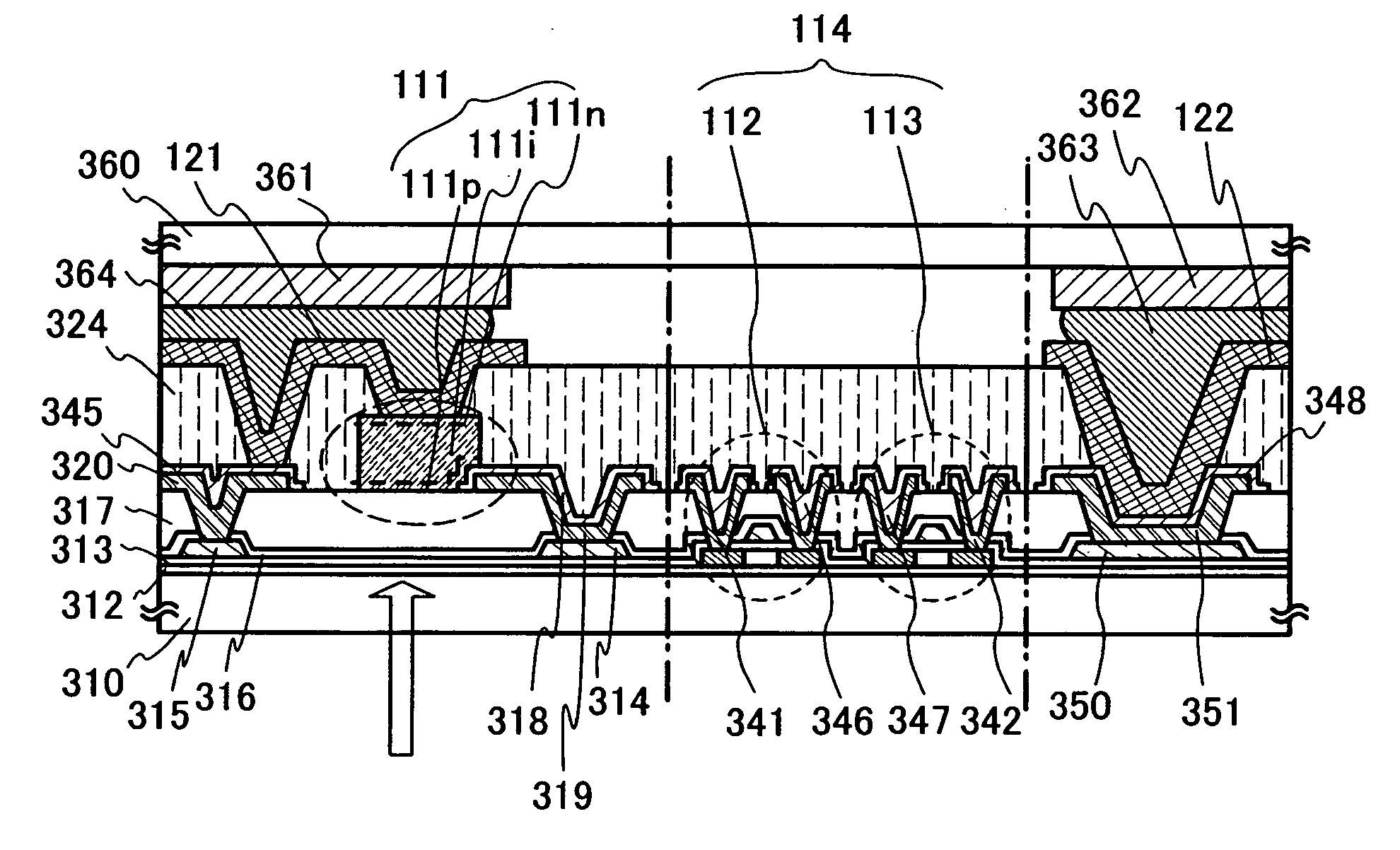
[0329]In this embodiment mode, a photoelectric conversion device having a structure different from those in Embodiment Modes 1 and 2 and a manufacturing method thereof are described with reference to FIGS. 14A to 14D, 15, 16A, 16B, 17, 18, 19, 20A, 20B, 21A, 21B, 22A, 22B, 23 to 27, 28A, 28B, 36, and 37.

[0330]First, an insulating film 1102 is formed over a substrate 1101. As the substrate 1101, a glass substrate, a quartz substrate, a ceramic substrate, a silicon substrate, a metal substrate, a stainless-steel substrate, or the like can be used. Alternatively, a plastic substrate provided with a silicon film containing oxygen or nitrogen on either side may be used. In this embodiment mode, a glass substrate is used as the substrate 1101.

[0331]As the insulating film 1102, a film may be formed of silicon oxide, silicon oxide containing nitrogen, silicon nitride, silicon nitride containing oxygen, or a metal oxide material by a sputtering method or a plasma CVD method.

[0332]A metal fil...


PUM


Abstract

A photoelectric conversion device includes a light detection circuit which includes an optical sensor to output a current signal corresponding to illuminance and a current-voltage conversion circuit to convert the current signal output from the optical sensor into a voltage signal; an amplifier to amplify the voltage signal output from the light detection circuit; a comparison circuit to compare voltage output from the amplifier and reference voltage and output the result to a control circuit; and the control circuit to determine an illuminance range to be detected depending on the output from the comparison circuit and output a control signal to the light detection circuit. The current-voltage conversion circuit has a function of changing a resistance value in accordance with the control signal.

Description

BACKGROUND OF THE INVENTION[0001]1. Field of the Invention[0002]The present invention relates to a semiconductor device. In particular, the present invention relates to a semiconductor device including a photoelectric conversion element. In addition, the present invention relates to an electronic device using the semiconductor device.[0003]2. Description of the Related Art[0004]A number of photoelectric conversion devices generally used for sensing an electromagnetic wave are known, and for example, a photoelectric conversion device having sensitivity in ultraviolet rays to infrared rays is collectively referred to as an optical sensor. An optical sensor having sensitivity in a visible light region with a wavelength of 400 to 700 nm is particularly referred to as a visible light sensor, and a large number of visible light sensors are used for devices which need illuminance adjustment, on / off control, or the like depending on human living environment.[0005]In particular, in a display...

Claims


Application Information

Patent Timeline
IPC IPC(8): G09G3/36H03F3/08
CPCG09G3/3413G09G3/3622G09G3/3648G09G2310/0235G09G2310/06G09G2320/0223H03F3/082G09G2320/0633G09G2320/064G09G2320/066G09G2340/16G09G2360/144G09G2320/0252H01L31/101H01L31/09
Inventor YOSHIDA, YASUNORI
Owner SEMICON ENERGY LAB CO LTD
Why Eureka
Try Eureka