Solar cell and solar cell module

a solar cell and solar cell technology, applied in the field of solar cell and solar cell modules, can solve the problems of easy cracks and brittle fractures inside such a collector electrode, and the collector electrode formed by the use of sintering conductive paste is not easily plastically deformed, and achieves the effect of improving reliability

Inactive Publication Date: 2008-08-21
PANASONIC INTELLECTUAL PROPERTY MANAGEMENT CO LTD
View PDF9 Cites 133 Cited by
  • Summary
  • Abstract
  • Description
  • Claims
  • Application Information

AI Technical Summary

Benefits of technology

[0013]An aspect of the invention provides a solar cell and a solar cell module with en...

Problems solved by technology

The collector electrodes formed by use of the sintering conductive paste are not easily plastically deformable and are brittle in nature.
Cracks and brittle fractures easily occur inside such a collector electrode when stress is applied.
Therefore, cracks and brittle fractures may occur inside the collector electrodes due to an influence of the stress generated on the interface between the tab and the ...

Method used


Image

  • Solar cell and solar cell module
  • Solar cell and solar cell module
  • Solar cell and solar cell module

Examples


example 1

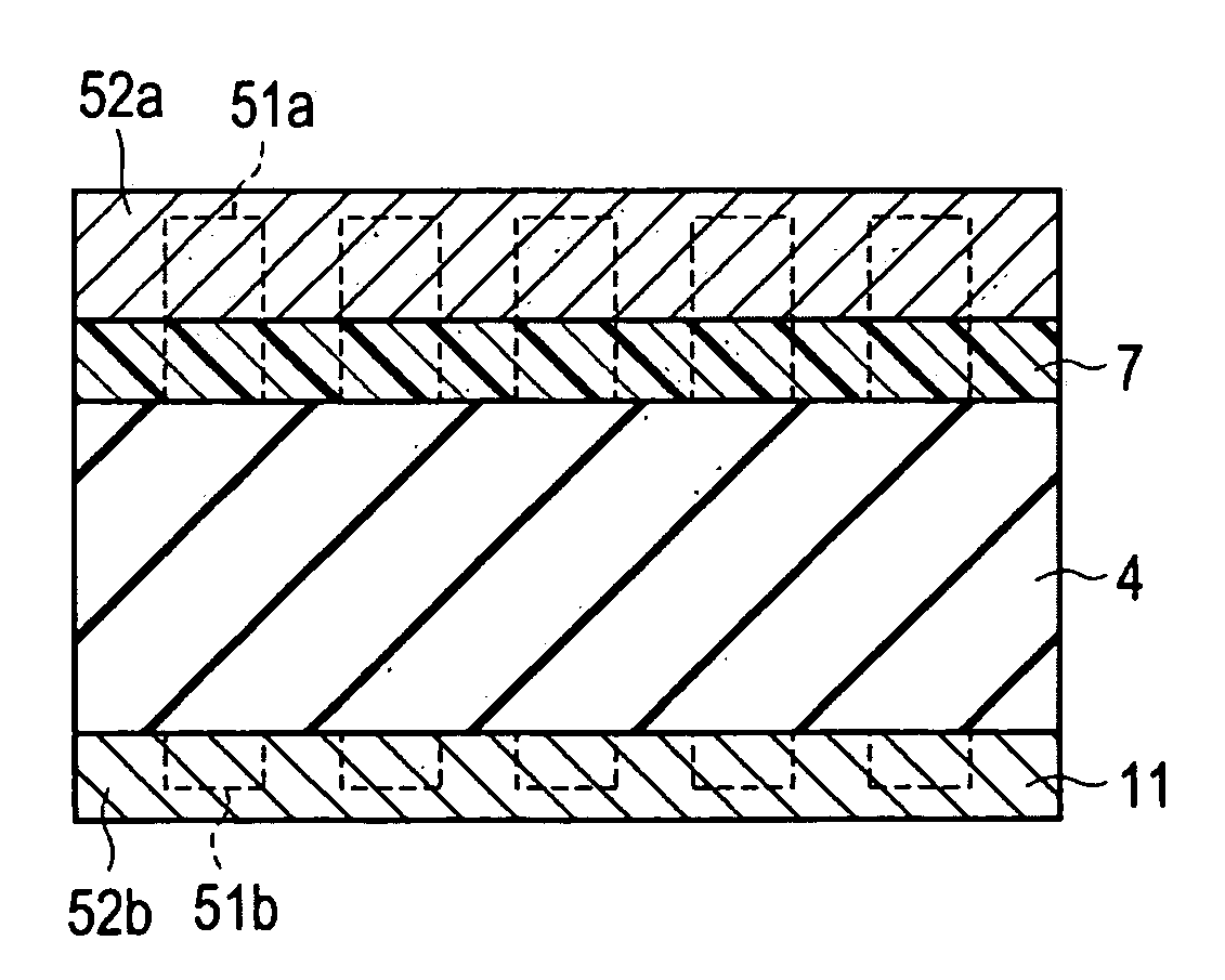
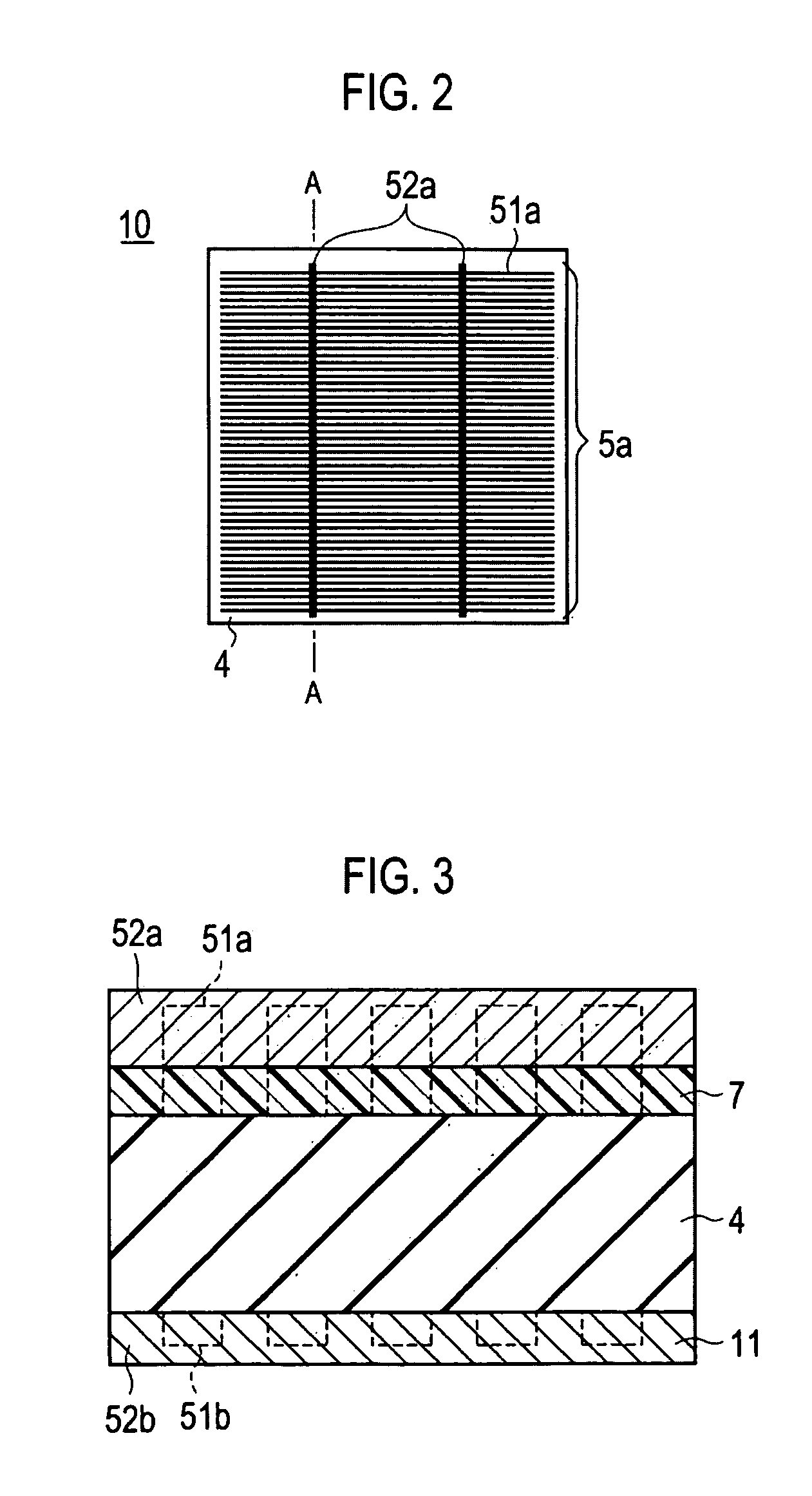
[0065]Next, concrete example of this embodiment is described. First, an n-type semiconductor layer is formed, by diffusing P with the thermal diffusion method, on an acceptance surface of a 125-mm square p-type polycrystalline silicon substrate. Moreover, a p+-type diffused layer is formed by diffusing Al with the thermal diffusion method, on a back surface side of the p-type polycrystalline silicon substrate. Next, a SiN film (the anti-reflective film) is formed, by a plasma CVD method, on an acceptance surface of the n-type semiconductor layer.

[0066]Then, silver paste is coated into a line shape, by the screen printing method, on the acceptance surface side of the SiN film, as well as on the back surface side on the p+-type diffused layer. The silver paste used therein is formed by blending: 70 wt % of silver powder having grain sizes of 1 μmφ; 5 wt % of PbO—B2O3-based glass frit; and 25 wt % of an organic vehicle prepared by dissolving ethylcellulose into terpineol. Meanwhile, as...

example 2

[0071]Here, different features from the manufacturing method of Example 1 is described.

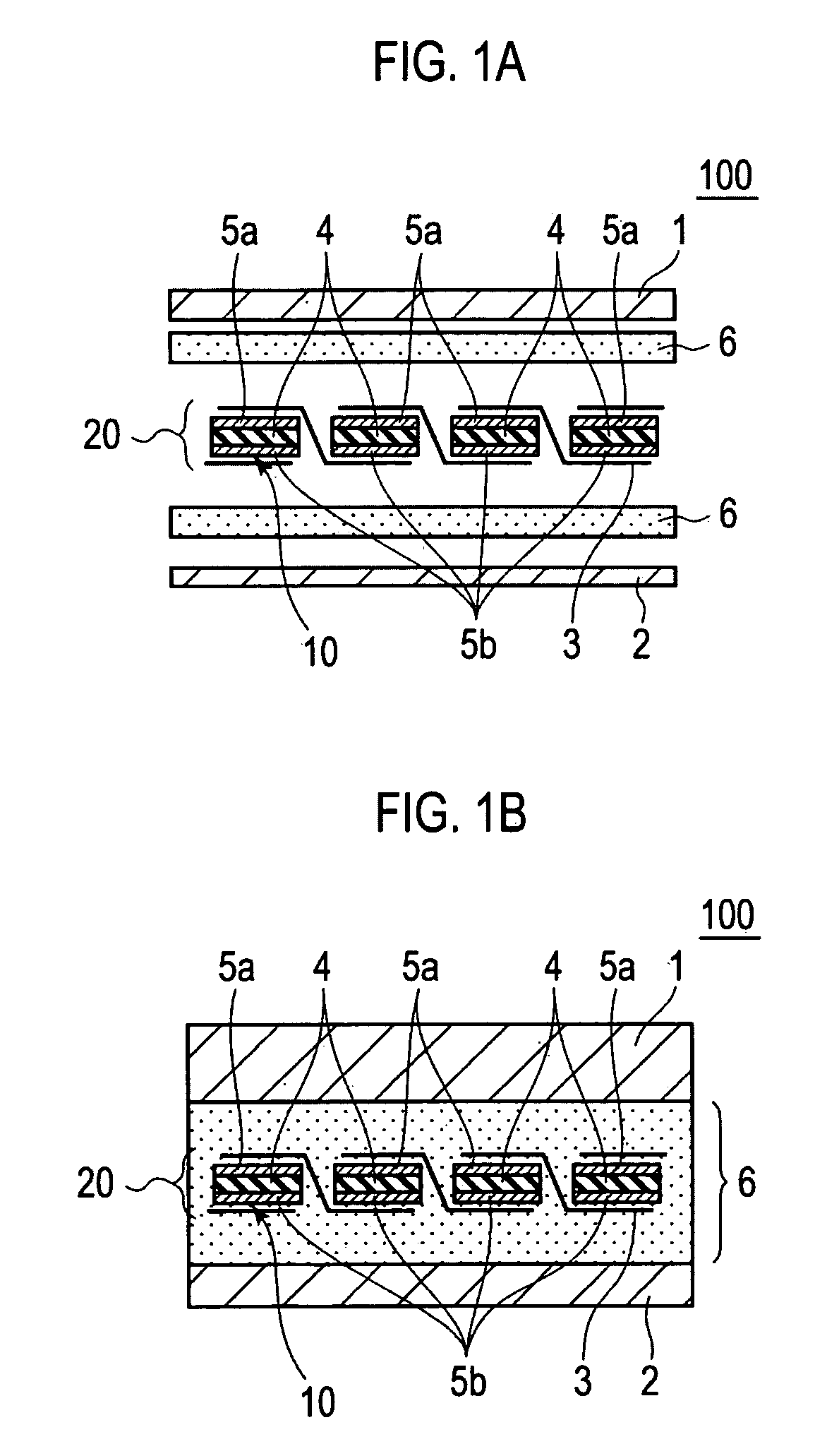
[0072]In Example 2, thermosetting resin containing conductive particles is used as the conductive adhesive instead of the solder. To be more precise, the thermosetting resin having a width of 1.5 mm and a thickness of 20 μm is printed on the acceptance surface bus-bar electrodes and the back surface sub-bar electrodes with the screen sprinting method. The conductive adhesive is prepared by mixing fast curing epoxy resin with 5 wt % of silicone resin, and then by mixing 3 wt % of spherical Ni powder (grain sizes of 15 μmφ) therewith.

[0073]Next, a first end of each tab is disposed above the acceptance surface bus-bar electrode of a crystalline solar cell, while a second end thereof is disposed below the back surface bus-bar electrode of the adjacent crystalline solar cell. In the state of sandwiching the solar cells with the tabs, the tabs and the bus-bar electrodes are bonded together by pressurizi...


PUM


Abstract

A photoelectric converter generates carriers by photoelectric conversion. A multiple finger electrodes are electrically coupled to the photoelectric converter. The finger electrodes collect carriers generated in the photoelectric converter. The finger electrodes contain a sintering conductive material as an essential ingredient. A bus-bar electrode is electrically coupled to the multiple finger electrodes. The bus-bar electrode collects the carriers from the finger electrodes. The bus-bar electrode contains a thermosetting conductive material as an essential ingredient.

Description

CROSS REFERENCE TO RELATED APPLICATIONS[0001]This application claims priority based on 35 USC 119 from prior Japanese Patent Application No. P2007-038650 filed on Feb. 19, 2007, the entire contents of which are incorporated herein by reference.BACKGROUND OF THE INVENTION[0002]1. Field of the Invention[0003]The invention relates to a solar cell and a solar cell module. More specifically, the invention relates to: a solar cell including a photoelectric converter, a finger electrode and a bus-bar electrode, the electrodes formed on the photoelectric converter; and a solar cell module including multiple solar batteries provided between a top surface protector and a back surface protector and electrically interconnected with wiring tabs.[0004]2. Description of Related Art[0005]Solar cells directly convert sunlight, which is clean and inexhaustibly supplied, into electricity. For this reason, solar cells are expected to be new energy sources.[0006]Each solar cell sheet generates an output...

Claims


Application Information

Patent Timeline
IPC IPC(8): H01L31/0224H01L31/04H01L31/042
CPCH01L31/022425Y02E10/50H01L31/048
Inventor YOSHIMINE, YUKIHIRO
Owner PANASONIC INTELLECTUAL PROPERTY MANAGEMENT CO LTD
Why Eureka
Try Eureka