

Semiconductor device
a technology of semiconductors and devices, applied in the direction of solid-state devices, inductances, basic electric elements, etc., can solve the problems of low yield and increased costs, and achieve the effect of increasing efficiency and inductance valu
- Summary
- Abstract
- Description
- Claims
- Application Information
AI Technical Summary
Benefits of technology
Problems solved by technology
Method used
Image

Examples
Embodiment Construction
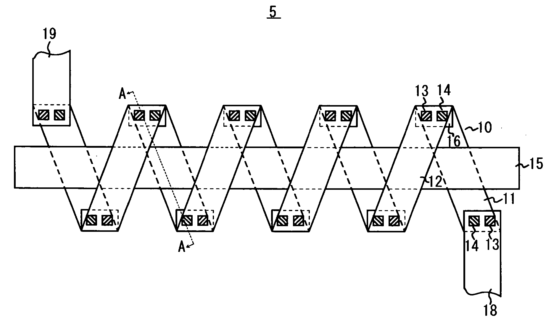
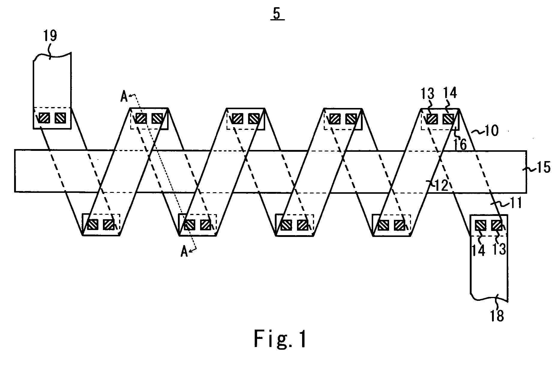
[0023]Preferred embodiments of the present invention will now be described with reference to the drawings. FIG. 1 is a plan view depicting an inductor 5 to be enclosed in a semiconductor device according to a preferred embodiment of the present invention. This semiconductor device preferably includes semiconductor elements, such as MOS transistors or bi-polar transistors, and first, second and third metal wire layers which are disposed at different positions in the thickness direction for electrically connecting the semiconductor elements. Inter-layer insulation films 22 and 23, to be described later, are formed between the first, second and third metal wire layers, respectively. The inductor 5 includes a core 15 which preferably has a substantially bar-shaped configuration at a portion of the second metal wire layer, which is positioned in the middle in the thickness direction, a plurality of first pieces 11 of the first metal wire layer, which is positioned at the bottom in the th...
PUM
| Property | Measurement | Unit |
|---|---|---|
| angle | aaaaa | aaaaa |
| thickness | aaaaa | aaaaa |
| angle | aaaaa | aaaaa |
Abstract
Description
Claims
Application Information