Two-phase programming of a flash memory

a flash memory and two-phase technology, applied in the field of flash memory, can solve the problems of reducing the useful life of the cell, imposing stress on the cell, and relatively slow process of programming an array of flash cells

Active Publication Date: 2007-02-13
WESTERN DIGITAL ISRAEL LTD
View PDF7 Cites 103 Cited by
  • Summary
  • Abstract
  • Description
  • Claims
  • Application Information

AI Technical Summary

Problems solved by technology

In the illustrated case of a SLC, and in the case of the highest voltage band of a multi-level cell (MLC, in which each of 2n voltage bands corresponds to one of the 2n possible patterns of n bits), too high a programming voltage imposes stress on the cell that reduces the cell's useful lifetime.
The use of small voltage increments implies that the programming of an array of flash cells is a relatively slow process.

Method used


Image

  • Two-phase programming of a flash memory
  • Two-phase programming of a flash memory
  • Two-phase programming of a flash memory

Examples


Embodiment Construction

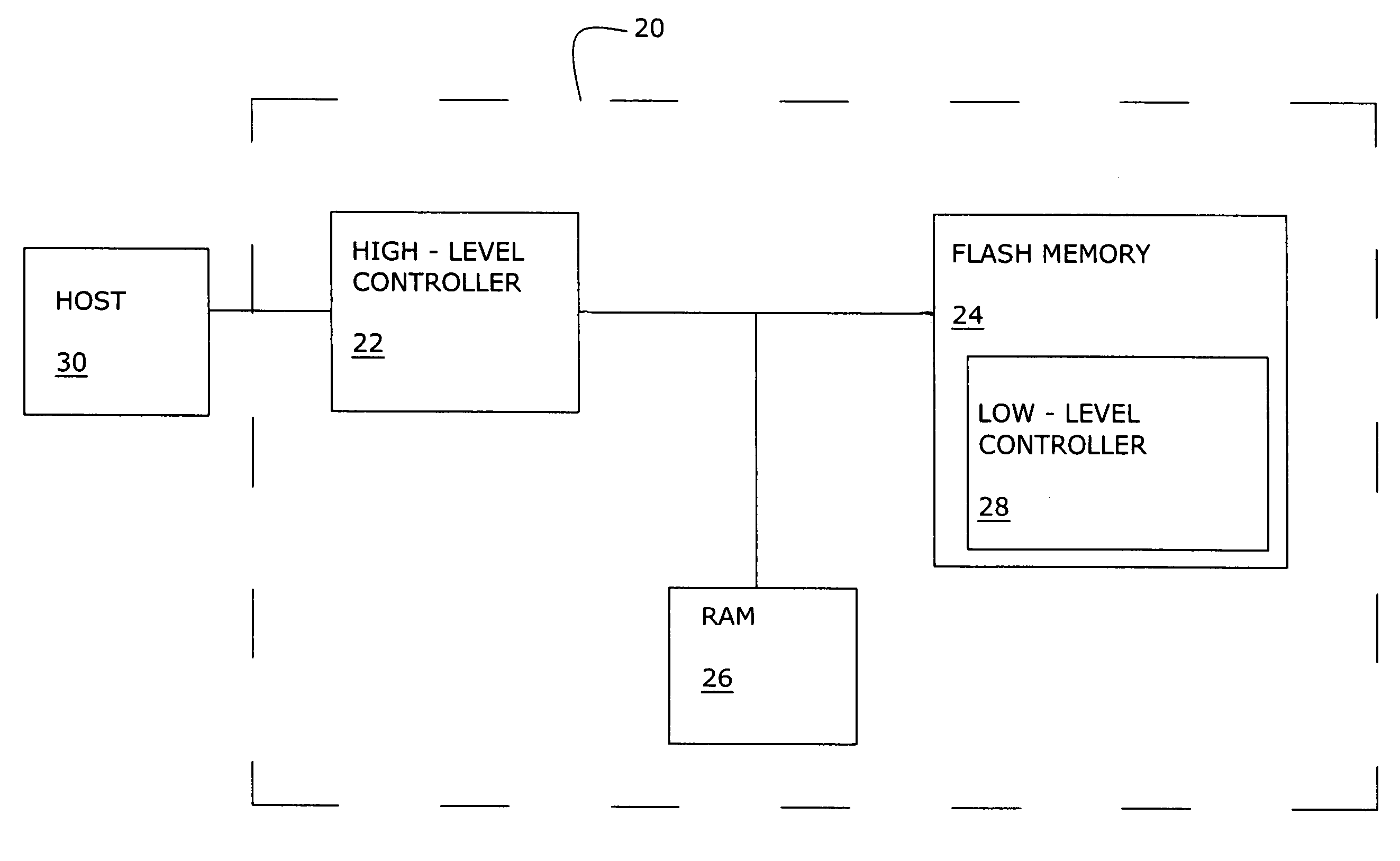
[0031]The present invention is of a method of programming a memory such as a flash memory, at an effective speed greater than that of prior art methods, with no loss in reliability.

[0032]The principles and operation of memory programming according to the present invention may be better understood with reference to the drawings and the accompanying description.

[0033]The present invention takes advantage of the fact that a host of a memory device such as a flash memory device typically exchanges data with the memory device only intermittently. For example, in the case of a digital camera with a detachable flash memory device, the user of the camera rarely if ever takes pictures at such a fast rate that the camera is continuously engaged in writing acquired digital images to the flash memory device. Nevertheless, a photographer sometimes desires to take a small number of pictures in quick succession, with the delay between successive pictures being as short as possible. This mandates t...


PUM


Abstract

A datum is stored in a memory by placing a memory cell in a first state that is indicative of the datum, and later placing the same or a different cell in a second state that is indicative of the same datum. If a different cell is placed in the second state, both cells are programmed to store the same number of bits, and then preferably the first cell is erased. Preferably, the first cell is placed in the first state by the application thereto of a first train of voltage pulses until the cell's threshold voltage exceeds a first reference voltage, and the first or second cell is placed in the second state by the application thereto of a second train of voltage pulses until the cell's threshold voltage exceeds a second reference voltage.

Description

[0001]This is a continuation-in-part of U.S. Provisional Patent Application No. 60 / 544,273, filed Feb. 10, 2004.FIELD AND BACKGROUND OF THE INVENTION[0002]The present invention relates to flash memories and, more particularly, to a method of increasing the effective programming speed of a flash memory with no loss in reliability.[0003]FIG. 1 illustrates the storage of a bit, either a zero bit or a one bit, in a cell of an electrically programmable memory (EPROM) such as a flash memory. For historical reasons, this process of storing data in a EPROM is called “programming” the EPROM. Specifically, the cell that is the subject of FIG. 1 is a single-level cell (SLC). Initially, the cell has a nominal threshold voltage V1 that represents a one bit. For example, after a block of a flash memory has been erased, all the cells have nominal threshold voltages V1. Because of unavoidable inaccuracies in the initializations of the cells, the actual threshold voltages are distributed around the ...

Claims


Application Information

Patent Timeline
Patent Type & Authority Patents(United States)
IPC IPC(8): G11C16/04G11C11/34G11C16/12G11C16/34
CPCG11C16/3468G11C16/12G11C16/10G11C16/04
Inventor RONEN, AMIRAVRAHAM, MEIR
Owner WESTERN DIGITAL ISRAEL LTD
Why Eureka
Try Eureka