Optical measurement device

a measurement device and optical technology, applied in the field of optical measurement devices, can solve the problems of deteriorating the bit error rate (ber), difficult to distinguish optical noise and signals from each other, and difficult to obtain an extremely small slit width, so as to achieve high resolution power and improve the accuracy of optical spectrum measuremen

Active Publication Date: 2007-05-01
FUJITSU LTD
View PDF5 Cites 8 Cited by
  • Summary
  • Abstract
  • Description
  • Claims
  • Application Information

AI Technical Summary

Benefits of technology

[0018]The present invention was created in view of the above circumstances, and an object thereof is to provide an optical measurement device which is capable of measuring an optical spectrum with high resolving power, without structurally decreasing the slit width, and thus is improved in accuracy of the optical spectrum measurement.

Problems solved by technology

Thus, in a system using an EDFA, amplified spontaneous emission (ASE) caused in the amplifier constitutes noise, which deteriorates the bit error rate (BER).
Especially, in 10-Gbps NRZ (Non-Return to Zero)-modulated WDM systems, the tails of adjacent signal spectra overlap with each other from the outset where the ch spacing is 50 GHz, making it more difficult to distinguish optical noise and signal from each other.
It is, however, difficult to obtain an extremely small slit width for structural reasons, giving rise to a problem that it is difficult to attain sufficiently high resolving power.

Method used


Image

  • Optical measurement device
  • Optical measurement device
  • Optical measurement device

Examples


first embodiment

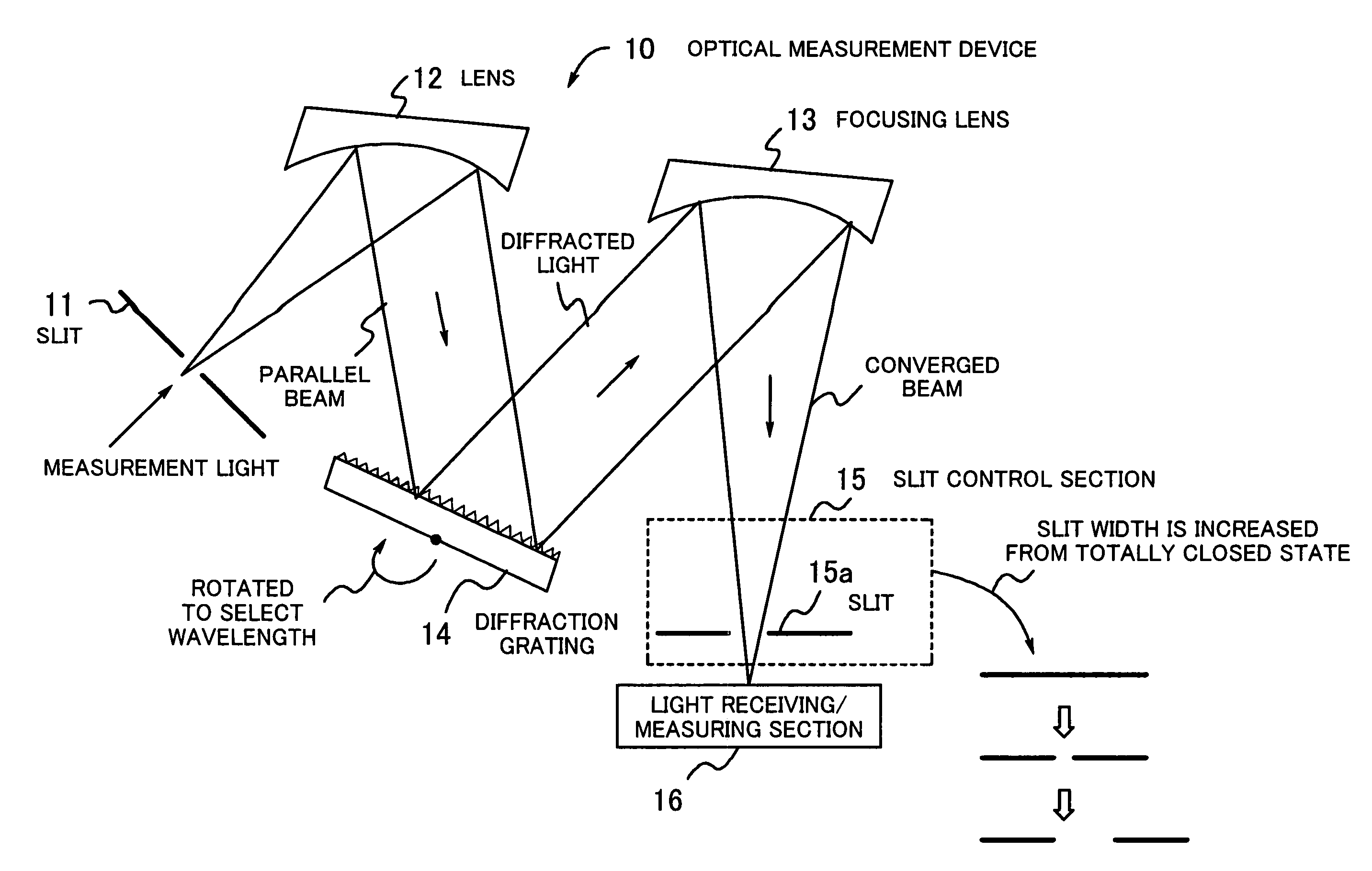
[0043]Embodiments of the present invention will be hereinafter described with reference to the drawings. FIG. 1 illustrates the principle of an optical measurement device according to the present invention. An optical measurement device 10, which is the present invention, comprises a slit 11, a lens 12, a focusing lens 13, a diffraction grating 14, a slit control section 15, and a light receiving / measuring section 16. The optical measurement device 10 corresponds to an optical spectrum analyzer and is used for the measurement of an optical spectrum. For example, the device is used to measure the optical power of light components contained in a certain frequency band of, for example, WDM light as measurement light to be measured, to obtain the OSNR.

[0044]After passing through the slit 11, the measurement light is reflected by the lens 12 and transformed into a parallel beam. The parallel beam then falls upon the diffraction grating 14 and is dispersed when emerging therefrom. Namely,...

second embodiment

[0090]Thus, in the second embodiment, the range of an optical spectrum bandwidth to be measured is set beforehand, and the received optical power is measured with the passing bandwidth varied within the set range. Accordingly, the measurement is performed after the range of measurement is narrowed to a certain degree, whereby the measurement efficiency can be improved (for example, only one channel of WDM signal can be easily selected so that the spectrum may be scanned by the slit within the band where the selected channel alone exists).

[0091]A third embodiment will be now described. FIG. 17 illustrates the third embodiment, and an optical measurement device 20 of this embodiment uses a VIPA (Virtually Imaged Phased Array) in place of the diffraction grating (VIPA is an optical component capable of dispersing light with extremely high resolving power and a schematic construction thereof will be described later with reference to FIG. 18). The use of a VIPA makes it possible to furth...


PUM


Abstract

An optical measurement device capable of improving optical spectrum measurement accuracy without the need to structurally decrease a slit width. A diffraction grating for dispersing measurement light into respective different wavelengths is rotated in a given direction to produce diffracted light of selected wavelengths. A focusing lens converges the diffracted light to produce a converged beam. A slit control section varies the slit width at a constant scan speed to open or close the slit, thereby varying the passing bandwidth for the converged beam. A light receiving / measuring section receives the light passed through the slit, obtains a level function indicative of the power level of the received light that varies with change in optical frequency, and differentiates the level function by the scan speed to reproduce the spectrum profile of the measurement light.

Description

CROSS-REFERENCE TO RELATED APPLICATIONS[0001]This application is based upon and claims the benefits of priority from the prior Japanese Patent Application No. 2004-206711, filed on Jul. 14, 2004, the entire contents of which are incorporated herein by reference.BACKGROUND OF THE INVENTION[0002](1) Field of the Invention[0003]The present invention relates to an optical measurement device, and more particularly, to an optical measurement device for measuring an optical spectrum.[0004](2) Description of the Related Art[0005]With recent increase in the amount of communicated information, large-capacity, low-cost optical fiber communication systems have been actively developed. To cope with increasing capacity, WDMs (Wavelength Division Multiplexers) for multiplexing a plurality of wavelengths for transmission have been researched and developed, making the degree of multiplexing higher and higher.[0006]Channel (ch) spacing, which is an index of the multiplexing degree, is standardized by...

Claims


Application Information

Patent Timeline
Patent Type & Authority Patents(United States)
IPC IPC(8): G01J3/28
CPCG01J3/04G01J3/18G01J3/1895G01J3/027G01J3/453
Inventor GOTO, RYOSUKESEKIYA, MOTOYOSHI
Owner FUJITSU LTD
Why Eureka
Try Eureka