Eureka AIR delivers breakthrough ideas for toughest innovation challenges, trusted by R&D personnel around the world.

Electronic device and method of manufacturing the same, circuit board, and electronic instrument

Inactive Publication Date: 2007-06-12
SEIKO EPSON CORP
View PDF19 Cites 5 Cited by
  • Summary
  • Abstract
  • Description
  • Claims
  • Application Information

AI Technical Summary

Benefits of technology

[0106]The side surface 74 could be formed when the wafer (such as a semiconductor wafer) 80 is cut apart, as shown in FIG. 9A. More specifically, a cutter (such as a dicing saw) 82 in which two slicing blades are connected at an angle like an angle milling cutter could be used to form a groove (such as a V-shaped groove) having inclined surfaces in

Problems solved by technology

With conventional chip-on-board (COB) mounting, the use of high temperatures require the substrate to have thermal resistivity, making it impossible to use a thermoplastic substrate.
This makes it difficult to use an inexpensive substrate.
In addition, since a semiconductor chip is subjected to external thermal or mechanical forces, it is difficult to avoid defects caused by the resultant stresses.
When wire bonding is used, there are restrictions on the lengths of wires, so a general-purpose substrate cannot be used.
Alternatively, if face-down bonding is used, it is necessary to use a special substrate that is matched to the layout of the electrodes of the semiconductor chip, so it is not possible to use a general-purpose substrate therefore.

Method used


Image

  • Electronic device and method of manufacturing the same, circuit board, and electronic instrument
  • Electronic device and method of manufacturing the same, circuit board, and electronic instrument
  • Electronic device and method of manufacturing the same, circuit board, and electronic instrument

Examples


Embodiment Construction

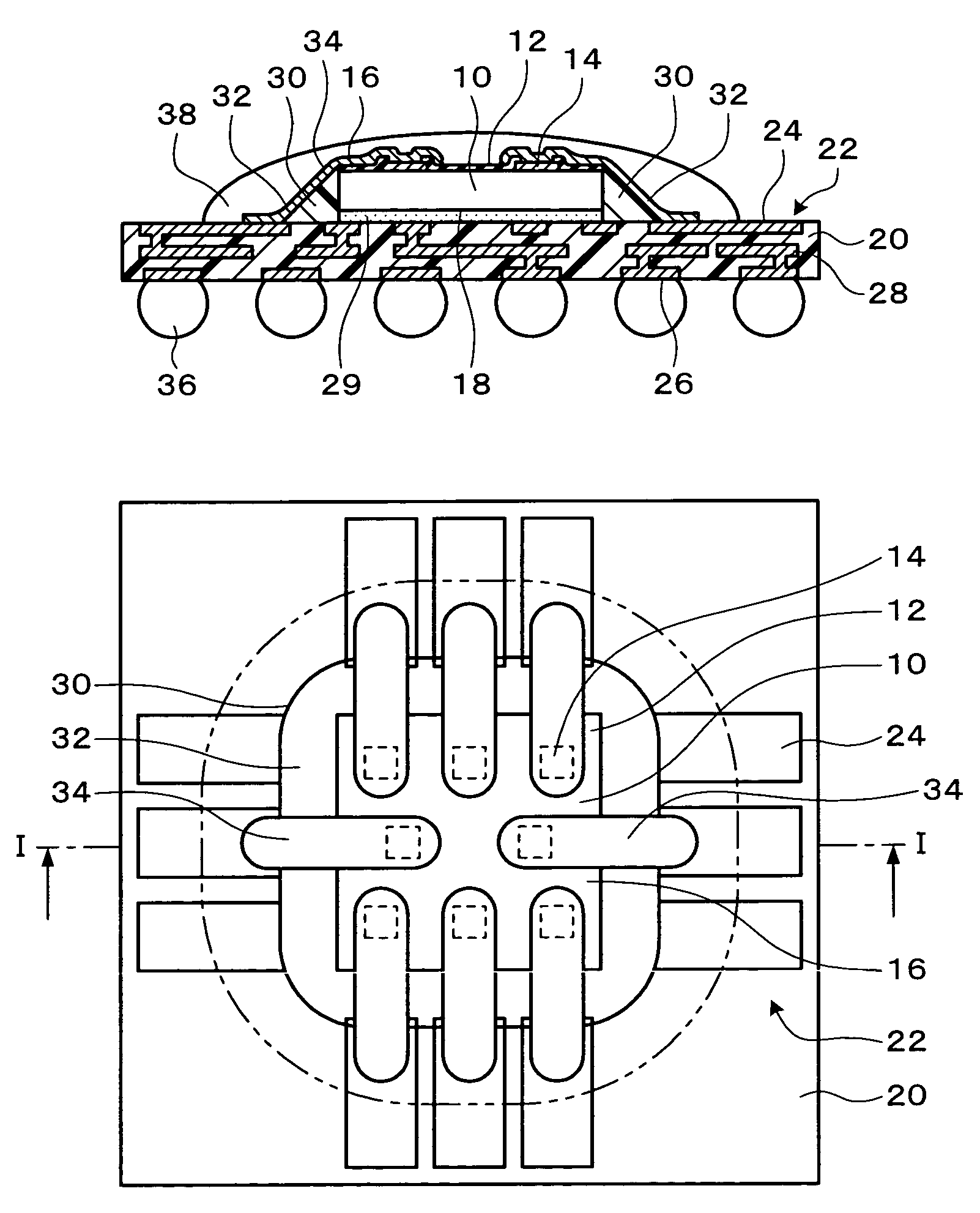
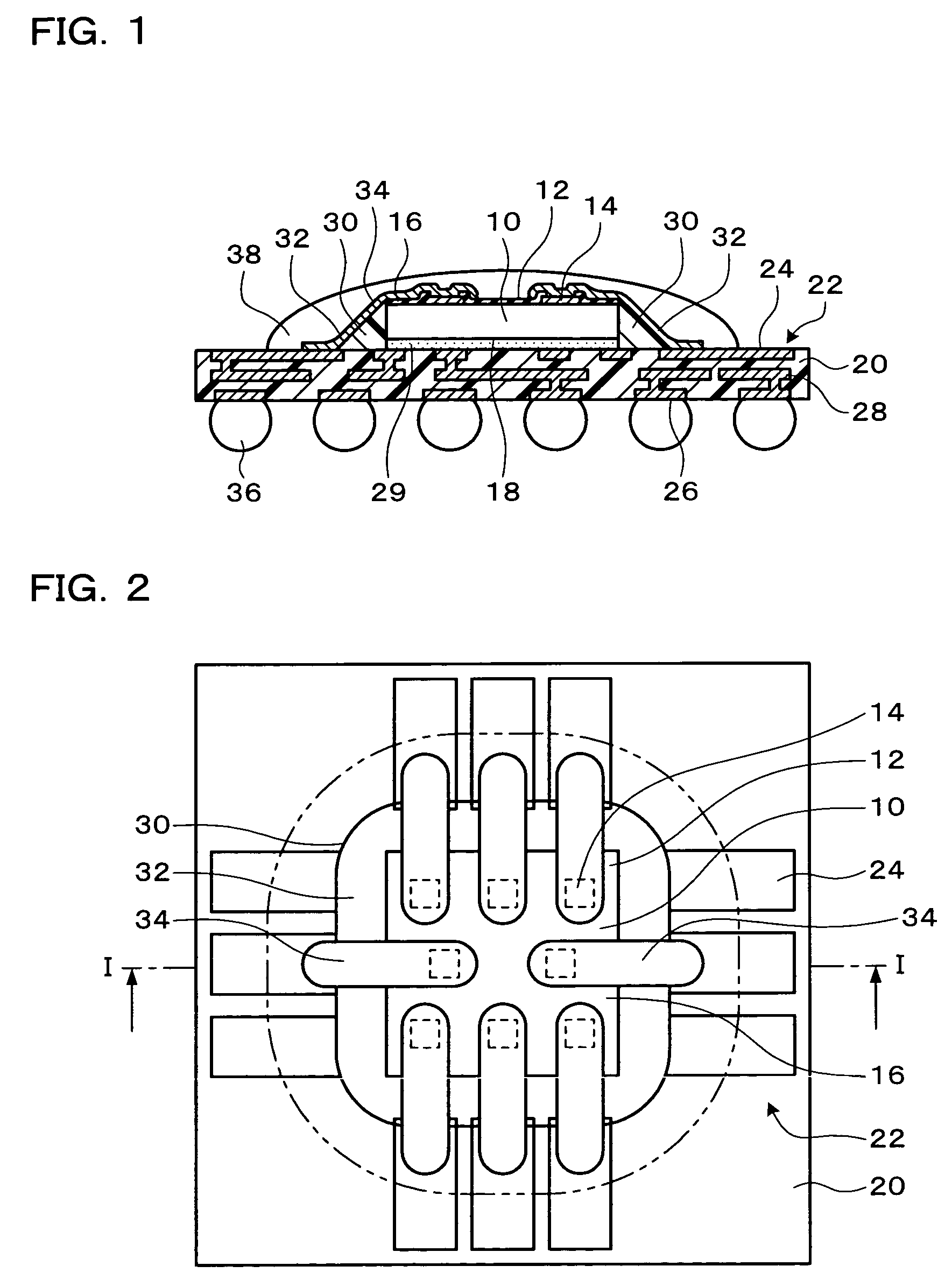
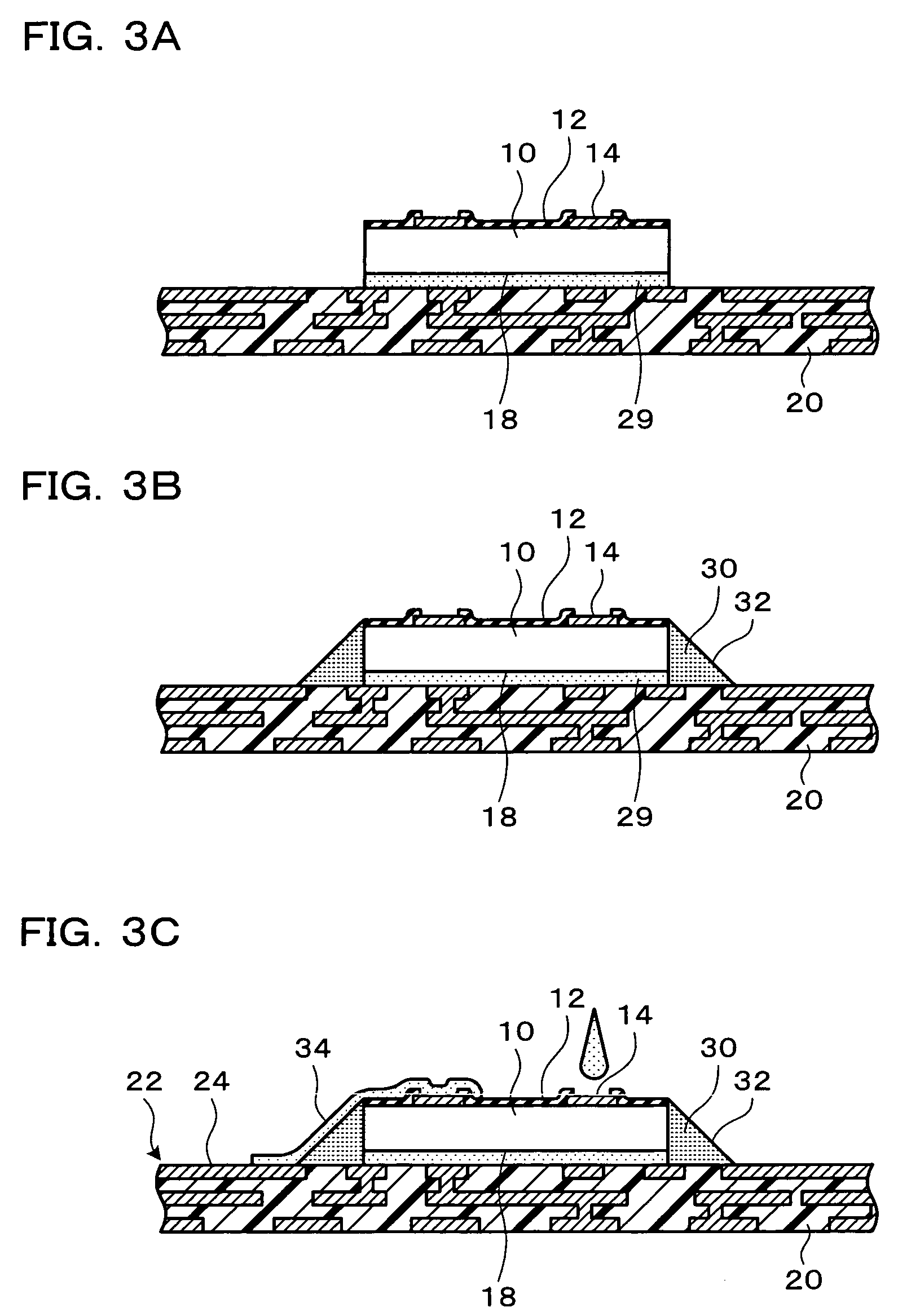
[0040]An embodiment of the present invention may reduce the requirement of thermal resistivity of the substrate, enable a reduction in the generation of stresses in the semiconductor chip, and make it possible to use a general-purpose substrate.

[0041](1) An electronic device according one embodiment of the present invention include:

[0042]a substrate on which an interconnect pattern is formed;

[0043]a chip component having a first surface on which an electrode is formed and a second surface opposite to the first surface, the chip component being mounted in such a manner that the second surface faces the substrate;

[0044]an insulating section formed of a resin and provided adjacent to the chip component; and

[0045]an interconnect which is formed to extend from above the electrode, over the insulating section and to above the interconnect pattern.

[0046]This embodiment of the present invention makes it possible to avoid the use of high-temperature heating such as that used for wire bonding...


PUM


Abstract

An electronic device includes: a substrate on which an interconnect pattern is formed; a chip component having a first surface on which an electrode is formed and a second surface opposite to the first surface, the chip component being mounted in such a manner that the second surface faces the substrate; an insulating section formed of a resin and provided adjacent to the chip component; and an interconnect which is formed to extend from above the electrode, over the insulating section and to above the interconnect pattern.

Description

[0001]Japanese Patent Application No. 2003-68279, filed on Mar. 13, 2003, is hereby incorporated by reference in its entirety.BACKGROUND OF THE INVENTION[0002]The present invention relates to an electronic device and a method of manufacturing the same, a circuit board, and also an electronic instrument.[0003]With conventional chip-on-board (COB) mounting, the use of high temperatures require the substrate to have thermal resistivity, making it impossible to use a thermoplastic substrate. This makes it difficult to use an inexpensive substrate. In addition, since a semiconductor chip is subjected to external thermal or mechanical forces, it is difficult to avoid defects caused by the resultant stresses. When wire bonding is used, there are restrictions on the lengths of wires, so a general-purpose substrate cannot be used. Alternatively, if face-down bonding is used, it is necessary to use a special substrate that is matched to the layout of the electrodes of the semiconductor chip, ...

Claims


Application Information

Patent Timeline
IPC IPC(8): H01L23/28H01L23/12H01L21/60H01L23/31H01L23/498H01L23/52H01L25/065H01L29/06
CPCH01L23/3128H01L23/3135H01L24/24H01L24/25H01L24/29H01L24/82H01L25/0657H01L23/49816H01L29/0657H01L2224/16H01L2224/24011H01L2224/24051H01L2224/24226H01L2224/24998H01L2224/2518H01L2224/291H01L2224/32225H01L2224/76155H01L2224/92H01L2224/92244H01L2924/01004H01L2924/01005H01L2924/01029H01L2924/0103H01L2924/01033H01L2924/01047H01L2924/0105H01L2924/01082H01L2924/10158H01L2924/14H01L2924/15311H01L2924/1532H01L2924/19041H01L2924/19042H01L2924/19043H01L2924/0132H01L2224/29H01L2224/2919H01L2924/01006H01L2924/01023H01L2924/014H01L2924/0665H01L2224/29101H01L2225/06517H01L2225/06524H01L2924/1517H01L2224/29111H01L2924/00013H01L2224/29299H01L2224/2929H01L2224/82007H01L2224/82102H01L2224/73267H01L2224/25175H01L2924/07802H01L2224/83H01L2224/82H01L2924/00H01L2924/01083H01L2924/00014H01L2224/29099H01L2224/29199H01L2224/05022H01L2224/05001H01L2224/05548H01L2224/05554H01L24/05H01L2224/05599H01L2224/05099
Inventor HASHIMOTO, NOBUAKI
Owner SEIKO EPSON CORP
Why Eureka
Eureka Blog
Learn More