
Semiconductor memory element and semiconductor memory device

a memory element and semiconductor technology, applied in the direction of information storage, static storage, digital storage, etc., can solve the problems of large circuits peripheral to memory cells, memory cells cannot be made smaller or driven at a lower voltage, and the thin film surrounding the floating gate cannot be as thin as desired

Inactive Publication Date: 2007-09-25
KK TOSHIBA
View PDF10 Cites 53 Cited by
  • Summary
  • Abstract
  • Description
  • Claims
  • Application Information

AI Technical Summary

Benefits of technology

The invention provides a semiconductor memory element comprising a first power-supply terminal, a second power-supply terminal, a MIS transistor with a gate, and two two-terminal variable resistor elements connected between the gate of the MIS transistor and the first and second power-supply terminals. The first and second variable resistor elements have resistances that change in response to a current flow and remain unchanged when the current is cut off. The semiconductor memory element also includes a control node connected to the gate of the MIS transistor. The technical effect of this invention is to provide a reliable and efficient semiconductor memory element that can change resistance in response to a current flow and remains stable even when the current is cut off.

Problems solved by technology

In the memory cell having a two-layered gate, however, the insulating film surrounding the floating gate cannot be as thin as desired because the floating gate must accumulate an electric charge.
Consequently, this memory cell cannot be made smaller or driven at a lower voltage.
Inevitably, the circuits peripheral to memory cells tend to become large.
As indicated above, a memory cell having a two-layered gate is disadvantageous in that the insulating film surrounding the floating gate cannot be as thin.
Inevitably, the memory cell cannot be made smaller or driven at a lower voltage.

Method used


Image

  • Semiconductor memory element and semiconductor memory device
  • Semiconductor memory element and semiconductor memory device
  • Semiconductor memory element and semiconductor memory device

Examples


first embodiment

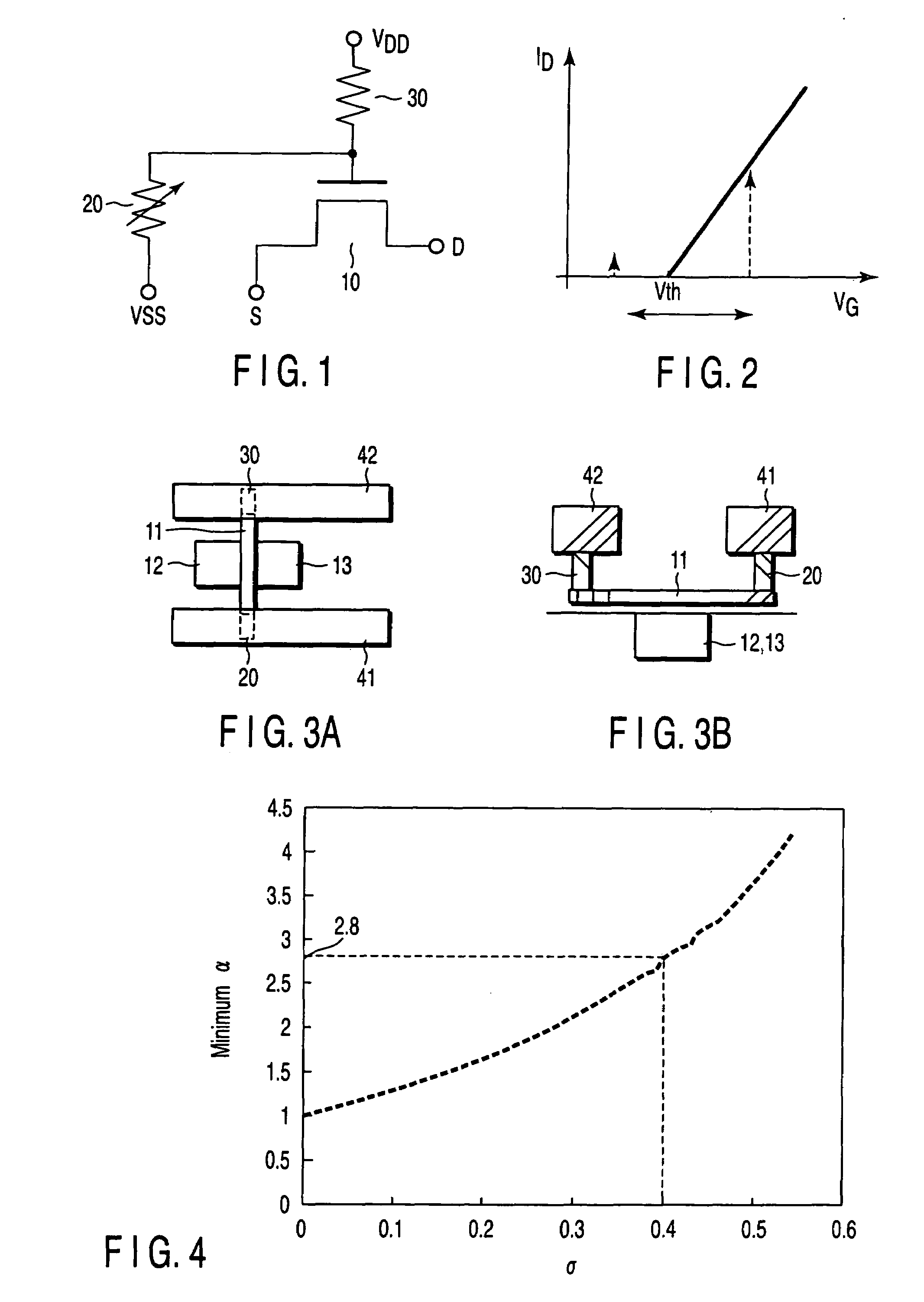
[0030]FIG. 1 is a circuit diagram showing a semiconductor memory element according to the first embodiment of the invention. The memory element shown here is one of the components (i.e., memory cells) that constitute a memory array.

[0031]As FIG. 1 shows, the memory element comprises a metal oxide semiconductor (MOS) transistor 10, a variable resistor element 20, and a resistor 30 (fixed resistor element). The variable resistor element 20 is connected at one end to the gate of the MOS transistor 10 and at the other end to the first power-supply terminal (e.g., ground terminal VSS terminal). The resistor 30 is connected at one end to the gate of the MOS transistor 10 and at the other end to the second power-supply terminal (e.g., power-supply terminal VDD). The variable resistor element 20 is made of, for example, phase-changing material. Its resistance varies with the temperature to which it is heated. More precisely, the variable resistor element 20 has either first resistance or se...

second embodiment

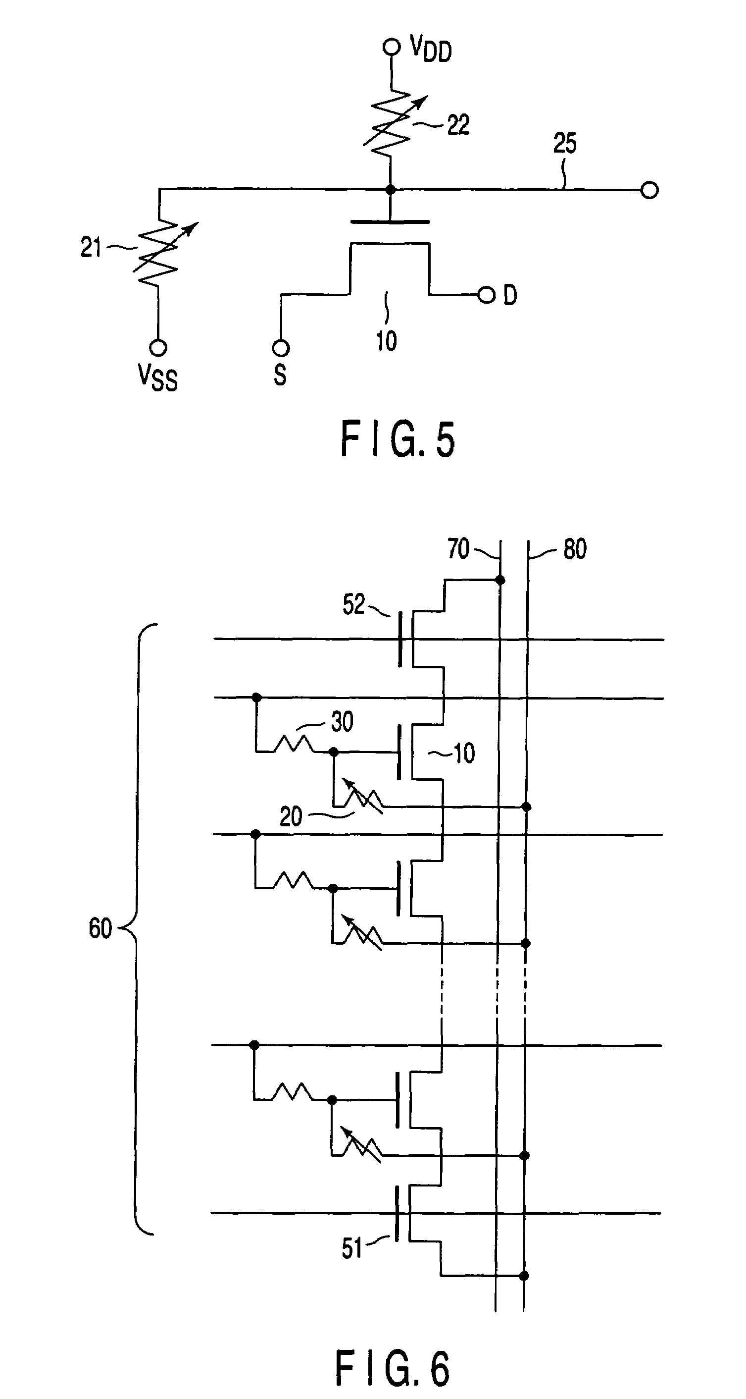
[0065]FIG. 5 is a circuit diagram that illustrates a semiconductor memory element according to the second embodiment of the present invention. More precisely, FIG. 5 depicts the structure of the smallest units (i.e., memory cells) that constitute a memory array.

[0066]The second embodiment differs from the first embodiment in that a control node 25 is provided as an additional component. As FIG. 5 shows, a first variable resistor element 21 is connected between the gate of a MOS transistor 10 and the first power-supply terminal (e.g., ground terminal VSS). And a second variable resistor element 22 is connected between the gate of the MOS transistor 10 and the second power-supply terminal (e.g., power-supply terminal VDD). The control node 25 is led from the gate of the MOS transistor 10.

[0067]In the first embodiment, the variable resistor element 20 and the resistor 30 are connected in series. In the second embodiment, the element 22 functions as a variable resistor element because t...

third embodiment

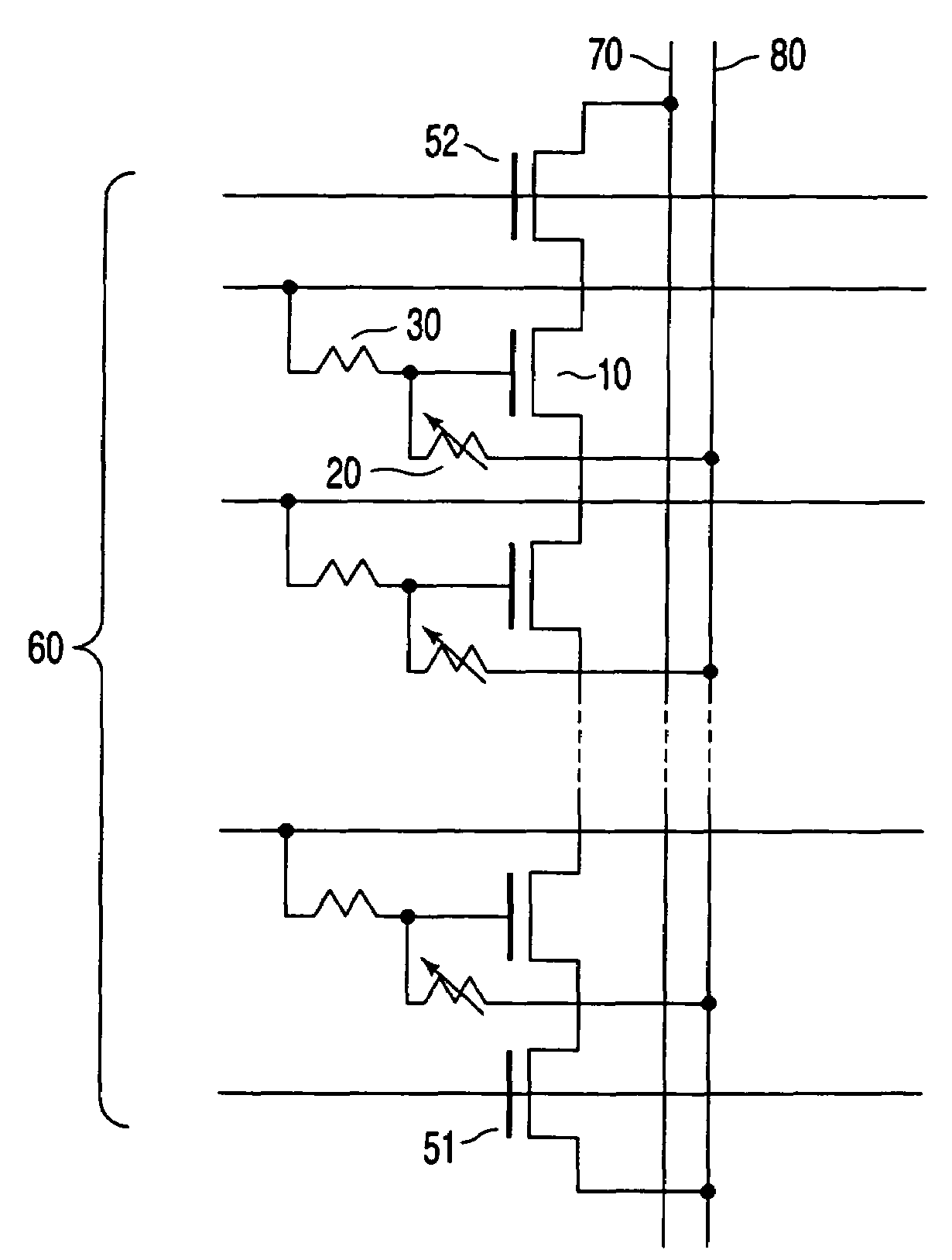
[0071]FIG. 6 is a circuit diagram showing a semiconductor memory device that is the third embodiment of the present invention.

[0072]More specifically, FIG. 6 depicts one of the blocks constituting a memory cell array, which includes memory cells of the type shown in FIG. 1. Memory cells of the type shown in FIG. 1 are connected in series, providing a series circuit. Two selection transistors are connected to the ends of this series circuit. The block shown in FIG. 6 and other identical blocks are arranged in rows and columns and are connected to one another, constituting the memory cell array.

[0073]As shown in FIG. 6, transistors 10 identical to the transistor included in the memory cell of FIG. 1 are connected in series, constituting a memory cell unit. The first selection transistor 51 is connected between the ground node of the memory cell unit and a source line 80. The second selection transistor 52 is connected between the power-supply node of the memory cell unit and a bit lin...


PUM


Abstract

A semiconductor memory element that stores data as a resistance difference. The memory element comprises a MIS transistor, a two-terminal variable resistor element, and a fixed resistor element. The MIS transistor has a gate. The two-terminal variable resistor element is connected between the gate of the MIS transistor and a first power-supply terminal. The variable resistor element has a resistance that changes in accordance with a current flowing in the variable resistor element or the direction in which the current flows and that remains unchanged when the current is made to stop flowing. The fixed resistor element is connected between the gate of the MIS transistor and a second power-supply terminal.

Description

CROSS-REFERENCE TO RELATED APPLICATIONS[0001]This application is based upon and claims the benefit of priority from prior Japanese Patent Application No. 2004-326812, filed Nov. 10, 2004, the entire contents of which are incorporated herein by reference.BACKGROUND OF THE INVENTION[0002]1. Field of the Invention[0003]The present invention relates to a semiconductor memory element that stores binary data 0 or 1 in the form of resistance. The invention relates also to a semiconductor memory device that has semiconductor memory elements of this type.[0004]2. Description of the Related Art[0005]Memory cells having a two-layered gate composed of a floating gate provided on a semiconductor substrate and a control gate provided on the floating gate are widely used as electrically programmable, nonvolatile semiconductor memory elements. Further, NAND-type semiconductor memory devices, each having memory cells of this type connected in series to acquire a large storage capacity, have been put...

Claims


Application Information

Patent Timeline
Patent Type & Authority Patents(United States)
IPC IPC(8): G11C11/00
CPCG11C11/16
Inventor YASUDA, SHINICHI
Owner KK TOSHIBA
Learn More