Plasma display panel (PDP) having phosphor layers in non-display areas

a technology of phosphor layer and display panel, which is applied in the direction of gas discharge vessel/container, electric discharge tube, gas-filled discharge tube, etc., can solve the problems of screen printing method, inconvenient mass production of pdps, and unnecessary consumption of time and materials

Inactive Publication Date: 2007-10-23
SAMSUNG SDI CO LTD
View PDF28 Cites 2 Cited by
  • Summary
  • Abstract
  • Description
  • Claims
  • Application Information

AI Technical Summary

Benefits of technology

[0010]It is also an object of the present invention to provide a PDP which enables optimizing a process for applying a phosphor paste, and to achieve mass production of PDPs using a nozzle jet method.

Problems solved by technology

However, when fabricating high definition PDPs or PDPs having closed barrier ribs, there are many problems in using a screen printing method or the like due to a narrow pitch of the plasma discharge cells.
Also, although an inkjet method or a photolithography method has been developed and used, these methods may be not suitable for mass production of PDPs due to the complex production processes required.
However, this method has many problems, such as the unnecessary consumption of time and materials, when used with a conventional screen printing or photolithography method to produce PDPs.

Method used


Image

  • Plasma display panel (PDP) having phosphor layers in non-display areas
  • Plasma display panel (PDP) having phosphor layers in non-display areas
  • Plasma display panel (PDP) having phosphor layers in non-display areas

Examples


Embodiment Construction

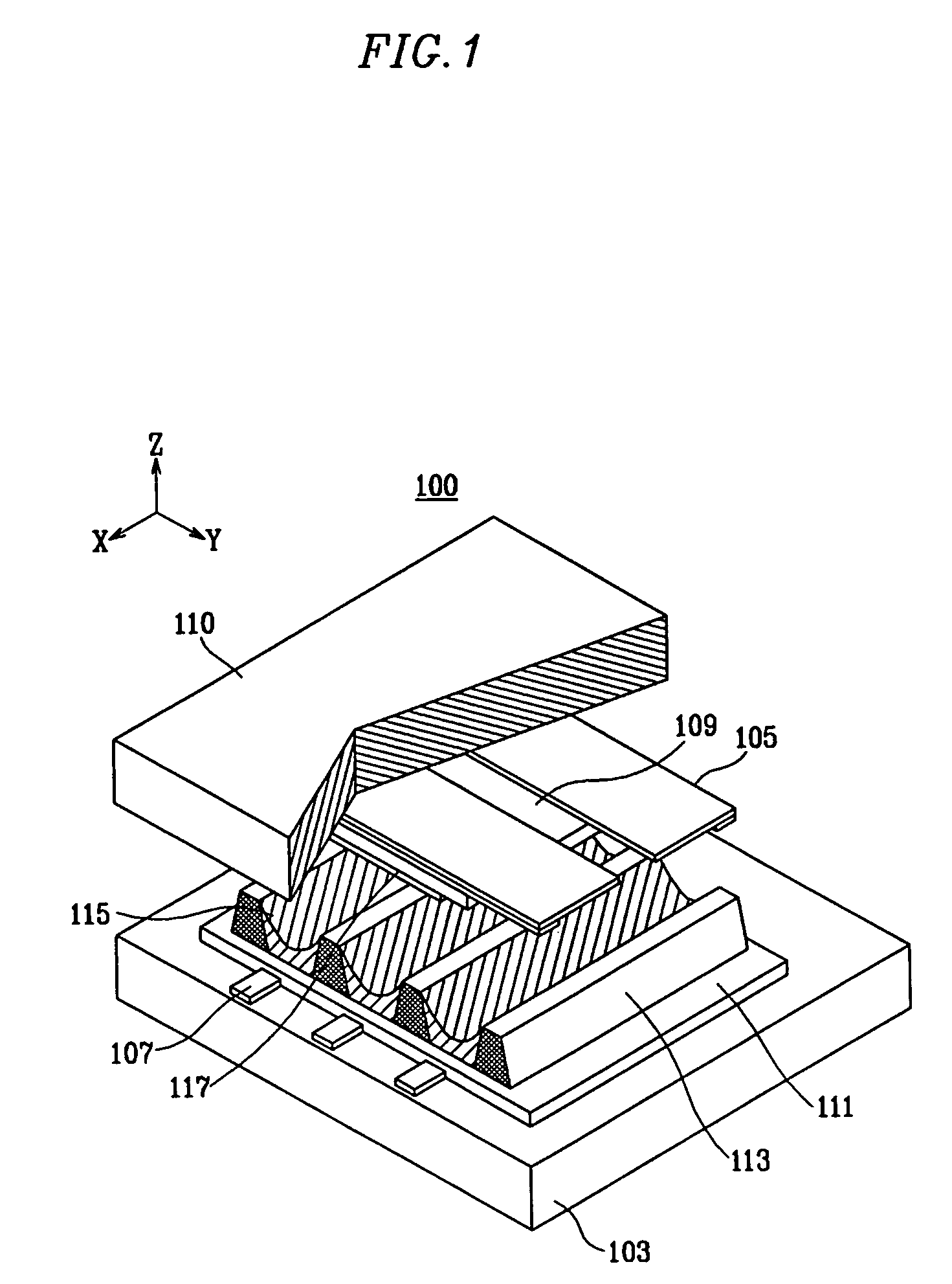
[0031]There are different types of PDPs including AC-PDPs, DC-PDPs, and hybrid PDPs. FIG. 1 is a partial exploded perspective view of an AC-PDP with a matrix barrier rib configuration. With reference to FIG. 1, an AC-PDP 100 includes a rear substrate 103, address electrodes 107 formed on the rear substrate 103, a dielectric layer 111 formed on an entire surface of the rear substrate 103 covering the address electrodes 107, a plurality of barrier ribs 113 formed over the dielectric layer 111 to maintain a constant discharge distance therebetween and to prevent the occurrence of cross-talk among the cells, and phosphor layers 115 formed between each of the neighboring barrier ribs 113. A plurality of display electrodes 105 are formed on a front substrate 110 and are arranged in pairs and spaced apart from each other and correspond to one discharge cell when they intersect the address electrodes 107 formed on the rear substrate 103. A dielectric layer 109 and a protective layer 117 are...


PUM


Abstract

A Plasma Display Panel (PDP) which enables optimization of a process to apply phosphor paste in order to achieve mass production using a nozzle jet method includes dummy areas structured in such a manner to determine whether or not applying conditions such as an ejecting pressure or the like are stable by measuring a depth of the applied layer after applying phosphor paste at a portion thereof in advance. The PDP includes: a first substrate and a second substrate opposing each other; address electrodes arranged on the first substrate; display electrodes arranged on the second substrate along a direction perpendicular to the address electrodes; barrier ribs arranged in a space between the first substrate and the second substrate to define a plurality of discharge cells, and phosphor layers arranged in each of the discharge cells.

Description

CLAIM OF PRIORITY[0001]This application makes reference to, incorporates the same herein, and claims all benefits accruing under 35 U.S.C. §119 from an applications entitled PLASMA DISPLAY PANEL earlier filed in the Korean Intellectual Property Office on 13 Nov. 2003 and 27 Nov. 2003 and there duly assigned Serial Nos. 10-2003-0080282 and 10-2003-0085117 respectively.BACKGROUND OF THE INVENTION[0002]1. Field of the Invention[0003]The present invention relates to a plasma display panel, and more particularly, to a plasma display panel having phosphor layers disposed differently on display areas and non-display areas thereof. The present invention also relates to a method of manufacturing a plurality of plasma display panels on one base plate.[0004]2. Description of the Related Art[0005]Generally, a plasma display panel, referred to hereinafter as a “PDP”, displays images based on a plasma discharge. When voltages are applied to electrodes arranged at discharge regions of the PDP, a p...

Claims


Application Information

Patent Timeline
Patent Type & Authority Patents(United States)
IPC IPC(8): H01J17/49
CPCH01J11/12H01J11/42H01J2211/368
Inventor JEON, BYUNG-SOO
Owner SAMSUNG SDI CO LTD
Why Eureka
Try Eureka