Organic electroluminescent device with HIL/HTL specific to each RGB pixel

an electroluminescent device and pixel specific technology, applied in the direction of discharge tube/lamp details, luminescent screen of discharge tube, natural mineral layered products, etc., can solve the problems of inability to obtain optimal light-emitting characteristics and inability to form organic el elements having optimal light-emitting conditions, etc., to achieve better light-emitting characteristics and better display characteristics

Inactive Publication Date: 2007-11-13
SEIKO EPSON CORP
View PDF7 Cites 5 Cited by
  • Summary
  • Abstract
  • Description
  • Claims
  • Application Information

AI Technical Summary

Benefits of technology

[0012]Since hole injection / transport properties of the hole injection / transport layers can be adjusted so as to correspond to materials for forming, for example, the light-emitting layers, it is possible to obtain optimal light-emitting characteristics for the individual organic EL elements.
[0047]According to the electronic apparatus, the organic EL device having better light-emitting characteristics for the individual organic EL elements is included as a display unit, so that it is possible to obtain better display characteristics.

Problems solved by technology

However, in the aforementioned organic EL device, particularly, an organic EL device for displaying full colors, since the light-emitting layers are composed of different materials for every color, optimal light-emitting characteristics cannot be obtained.
But, in this case, the hole injection / transport layers are formed commonly to the light-emitting layers composed of the different materials, and the electron injection / transport layers are not provided for all the colors.
Therefore, organic EL elements having optimal light-emitting conditions cannot be formed.

Method used


Image

  • Organic electroluminescent device with HIL/HTL specific to each RGB pixel
  • Organic electroluminescent device with HIL/HTL specific to each RGB pixel
  • Organic electroluminescent device with HIL/HTL specific to each RGB pixel

Examples


Embodiment Construction

[0059]Now, the present invention will be described in detail.

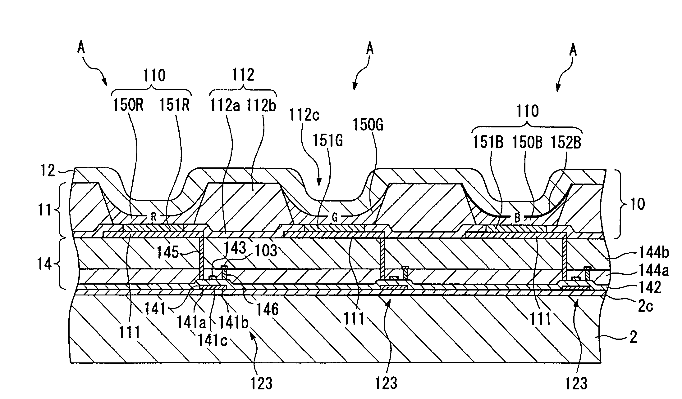
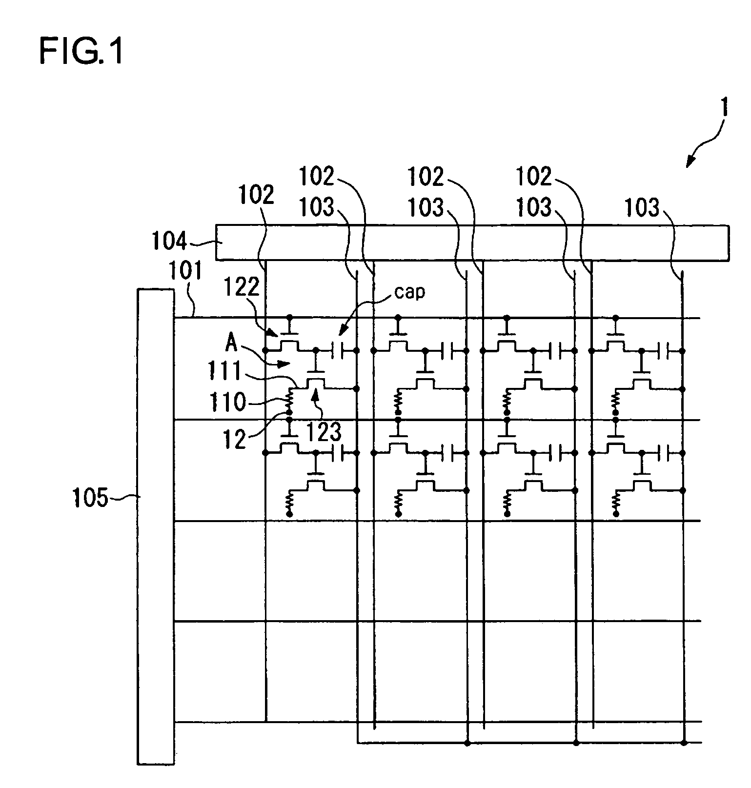
[0060]FIGS. 1 and 2 illustrate an active matrix display apparatus for full color display to which an organic EL device according to an embodiment of the present invention is applied. In the figures, reference numeral 1 denotes the organic EL device.

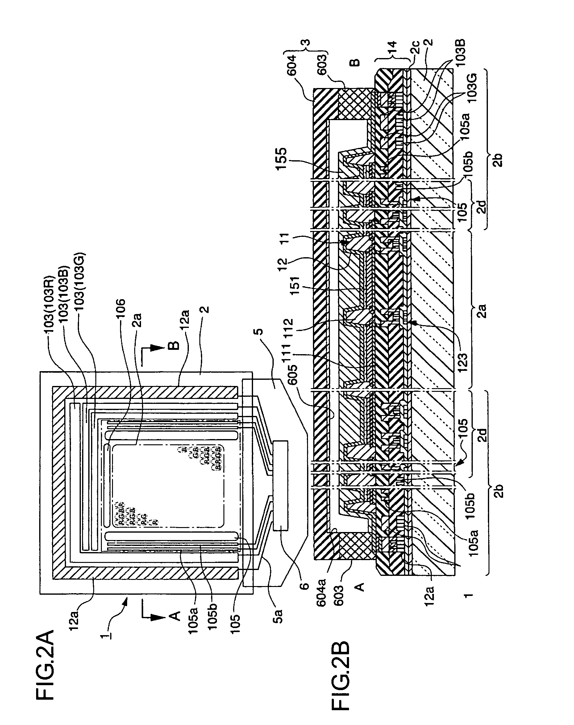
[0061]FIG. 1 is a schematic plan view showing a wiring structure of the organic EL device 1 according to the embodiment. FIG. 2 illustrates a schematic plan view and a schematic sectional view showing the organic EL device 1 according to the embodiment.

[0062]As shown in FIG. 1, the organic EL device 1 comprises wiring lines including a plurality of scan lines 101, a plurality of signal lines 102 intersecting the scan lines 101, and a plurality of power lines 103 extending parallel to the signal lines 102, and pixel regions A are formed at intersections of the scan lines 101 and the signal lines 102.

[0063]A data driving circuit 104 comprising a shift register, a level shifter, a ...


PUM

PropertyMeasurementUnit
mean particle diametersaaaaaaaaaa
work functionaaaaaaaaaa
thicknessaaaaaaaaaa

Abstract

An organic EL device comprises a plurality of organic EL elements, each of which has a pair of electrodes and functional layers including at least a light-emitting layer between the electrodes. With respect to components other than the light-emitting layer, the structure of the functional layer in one organic EL element among the organic EL elements is different from those of the functional layers in other organic EL elements.

Description

RELATED APPLICATIONS[0001]This application claims priority to Japanese Patent Application No. 2003-290653 filed Aug. 8, 2003 which is hereby expressly incorporated by reference herein in its entirety.BACKGROUND[0002]1. Technical Field[0003]The present invention relates to an organic EL device capable of improving characteristics of individual organic EL elements and display characteristics, a method of manufacturing the organic EL device, and an electronic apparatus.[0004]2. Background Art[0005]Recently, organic electroluminescent elements (hereinafter, referred to as organic EL elements) using organic materials functioning as light-emitting layers have been developed as self-emitting display elements. In an organic EL device having a plurality of the organic EL elements, functional materials for forming functional layers such as light-emitting layers and carrier injection / transport layers, that is, hole injection / transport layers or electron injection / transport layers, has become o...

Claims


Application Information

Patent Timeline
Patent Type & Authority Patents(United States)
IPC IPC(8): H01J63/04H01L51/50C09K11/06H01L27/32H01L51/00H05B33/00H05B33/02H05B33/10H05B33/14H05B33/20H05B33/22H05B33/26
CPCH01L27/3211H01L51/5048H01L51/0037H01L27/3244H10K59/35H10K59/12H10K85/1135H10K50/14H05B33/14H05B33/26
Inventor SEKI, SHUNICHIUCHIDA, MASAHIRO
Owner SEIKO EPSON CORP
Why Eureka
Try Eureka