Plasma display panel

a technology of display panel and plasma, which is applied in the direction of gas discharge vessel/container, electrode, gas-filled discharge tube, etc., can solve the problems of reducing the brightness of the screen, affecting the discharge operation, and reducing the dark room contrast of the screen, so as to achieve the effect of preventing the reflection of external light and improving screen contras

Inactive Publication Date: 2008-02-05
SAMSUNG SDI CO LTD
View PDF114 Cites 14 Cited by
  • Summary
  • Abstract
  • Description
  • Claims
  • Application Information

AI Technical Summary

Benefits of technology

[0018]In accordance with the present invention, a plasma display panel is provided that improves screen contrast by effectively preventing the reflection of external light from an outer surface of a front substrate while not causing any abnormalities in illumination in discharge cells.

Problems solved by technology

This reduces the dark room contrast of the screen.
This causes a decrease in the bright room contrast of the screen.
However, with the mounting of light shielding films on the inner surface of the front substrate and therefore adjacent to areas of discharge, the material in the light shielding films used to block light negatively affects the discharge operation so that discharge does not occur normally.
Further, the light shielding films are unable to prevent reflection from the outer surface of the front substrate.
This may cause problems (i.e., significant reflection) when the PDP is placed in a room using fluorescent lights or other such high-intensity lighting, thereby being unable to prevent a reduction in bright room contrast.
However, in the method utilizing gamma compensation described above, not all 255 sustain pulses needed for maximum green and red brightness are used.
Further, with the use of discharge cells of differing sizes, the likelihood of mis-discharge occurring increases, and a voltage margin, needed for stable driving, decreases.

Method used


Image

  • Plasma display panel
  • Plasma display panel
  • Plasma display panel

Examples


first embodiment

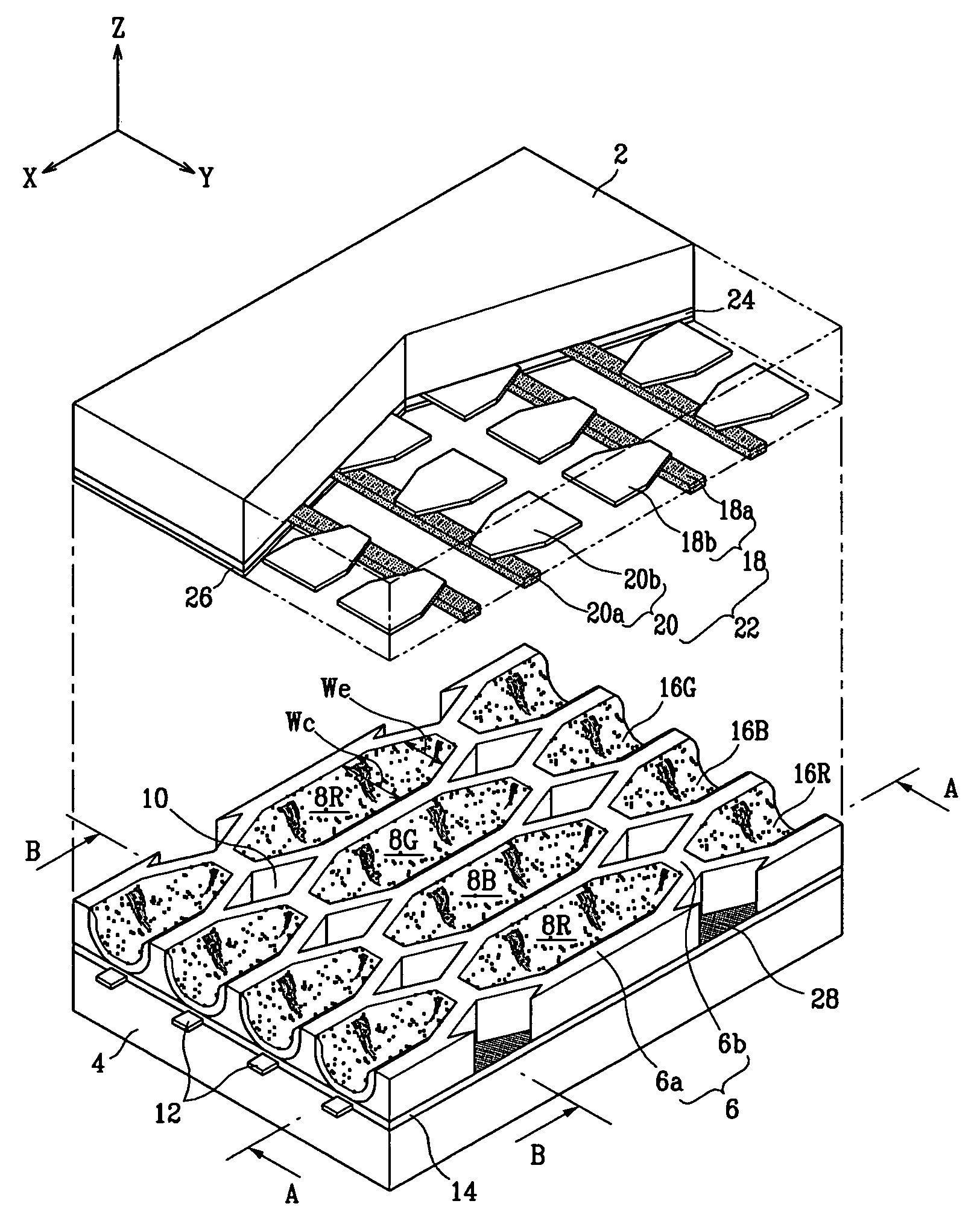
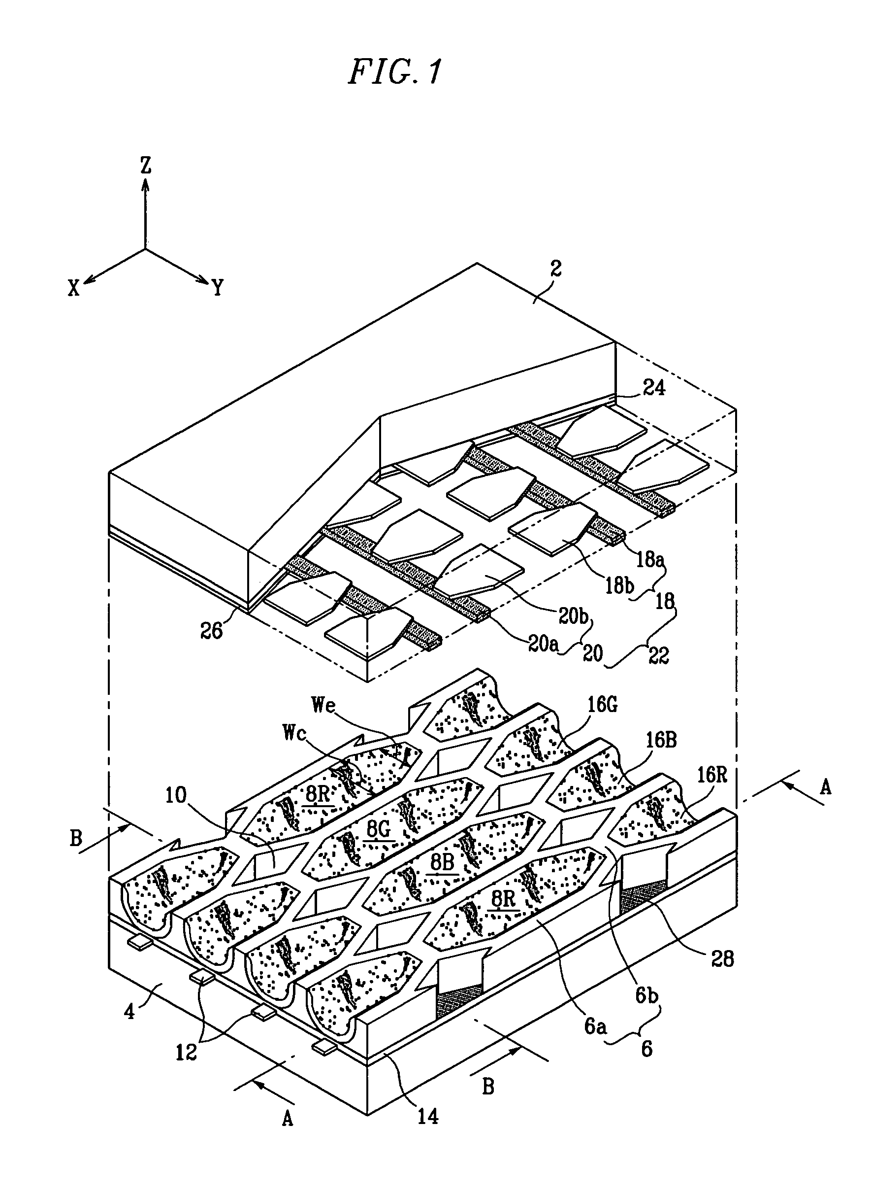
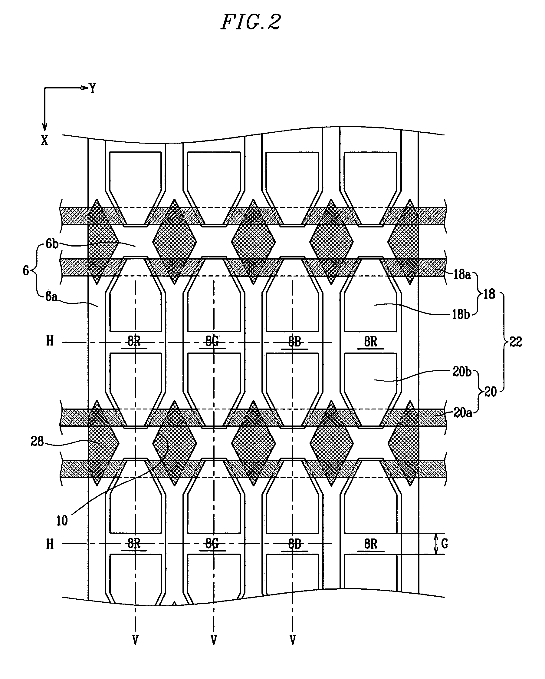
[0066]FIG. 1 is a partial exploded perspective view of a plasma display panel according to the present invention. FIG. 2 is a partial plan view of the plasma display panel of FIG. 1. FIG. 3 is a sectional view taken along line A-A of FIG. 1.

[0067]A plasma display panel (PDP) according to the first embodiment includes first substrate 2 and second substrate 4 provided substantially in parallel with a predetermined gap therebetween. Non-discharge regions 10 and discharge cells 8R, 8G, 8B are defined by barrier ribs 6 between first substrate 2 and second substrate 4.

[0068]A plurality of address electrodes 12 is formed along one direction (direction X in the drawings) on a surface of second substrate 4 opposing first substrate 2. As an example, address electrodes 12 are formed in a striped pattern with a uniform, predetermined interval between adjacent address electrodes 12. Dielectric layer 14 is formed on second substrate 4 covering address electrodes 12.

[0069]Barrier ribs 6 define the...

second embodiment

[0096]Dielectric layer 28 of the second embodiment includes tinted sections 28a that have the ability to absorb external light. Tinted sections 28a are formed corresponding to the location of non-discharge regions 10. This increases an overall external light absorbing area of the PDP. Tinted sections 28a may have one of black coloring or blue coloring, or a mixture of black and blue coloring. As a result of this configuration, areas corresponding to non-discharge regions 10 are darkened.

[0097]In one embodiment, the black coloring is realized by one of FeO, RuO2, TiO, Ti3O5, Ni2O3, CrO2, MnO2, Mn2O3, Mo2O3, and Fe3O4, or an any combination of these compounds; and the blue coloring is realized by one of Co2O3, CoO, and Nd2O3, or any combination of these compounds. In the case where tinted sections 28a include blue coloration so that non-discharge regions 10 exhibit a blue color, color purity and color temperature of the screen are improved.

[0098]Dielectric layer 28 including tinted se...

third embodiment

[0100]In the PDP discharge sustain electrodes 30, 31 respectively include bus electrodes 30a, 31a that are formed along a direction substantially perpendicular to a direction address electrodes 12 are and respectively include protrusion electrodes 30b, 31a that extend from bus electrodes 30a, 31b into areas corresponding to discharge cells 8R, 8G, 8B.

[0101]Distal ends of protrusion electrodes 30b, 31b are formed such that center areas along direction Y are indented and sections to both sides of the indentations are protruded. Therefore, in each of the discharge cells 8R, 8G, 8B, first discharge gap G1 and second discharge gap G2 of different sizes are formed between opposing protrusion electrodes 30b, 31b. That is, second discharge gaps G2 (or long gaps) are formed where the indentations of protrusion electrodes 30b, 31b oppose one another, and first discharge gaps G1 (or short gaps) are formed where the protruded areas to both sides of the indentations of protrusion electrodes 30b...


PUM


Abstract

A plasma display panel. A first substrate and a second substrate are provided opposing one another with a predetermined gap therebetween. Address electrodes are formed on the second substrate. Barrier ribs are mounted between the first substrate and the second substrate, the barrier ribs defining a plurality of discharge cells and a plurality of non-discharge regions. Phosphor layers are formed within each of the discharge cells. Discharge sustain electrodes are formed on the first substrate. The non-discharge regions are formed in areas encompassed by discharge cell abscissas and ordinates that pass through centers of each of the discharge cells. Also, external light absorbing members are formed between the second substrate and the barrier ribs layer at areas corresponding to locations of the non-discharge regions.

Description

CROSS REFERENCE TO RELATED APPLICATIONS[0001]This application claims priority to and the benefit of Korea Patent Applications: No. 2003-0041491 filed on Jun. 25, 2003, No. 2003-0044861 filed on Jul. 3, 2003, No. 2003-0050278 filed on Jul. 22, 2003, No. 2003-0052598 filed on Jul. 30, 2003, No. 2003-0053461 filed on Aug. 1, 2003, No. 2003-0073518 filed on Oct. 21, 2003 and No. 2003-0073519 filed on Oct. 21, 2003, all in the Korean Intellectual Property Office, the entire content of which are incorporated herein by reference.BACKGROUND OF THE INVENTION[0002](a) Field of the Invention[0003]The present invention relates to a plasma display panel (PDP), and more particularly, to a plasma display panel having a structure preventing the reflection of external light to improve screen contrast.[0004](b) Description of the Related Art[0005]A PDP is typically a display device in which vacuum ultraviolet rays generated by the discharge of gas occurring in discharge cells excite phosphors to real...

Claims


Application Information

Patent Timeline
Patent Type & Authority Patents(United States)
IPC IPC(8): H01J17/49H01J11/12H01J11/22H01J11/24H01J11/26H01J11/32H01J11/34H01J11/36H01J11/38H01J11/40H01J11/42H01J11/44H01J11/50
CPCH01J11/12H01J11/24H01J11/36H01J11/44H01J2211/245H01J2211/365H01J2211/444
Inventor WOO, SEOK-GYUNKIM, WOO-TAEKANG, KYOUNG-DOOYOO, HUN-SUKKWON, JAE-IKKWEON, TAE-JOUNGHEO, EUN-GI
Owner SAMSUNG SDI CO LTD
Why Eureka
Try Eureka