Optical device

Active Publication Date: 2020-12-24
FUJIFILM CORP
View PDF12 Cites 0 Cited by
  • Summary
  • Abstract
  • Description
  • Claims
  • Application Information

AI Technical Summary

Benefits of technology

The patent text describes an organic EL display device that uses an antireflection film to prevent external light from reflecting on the display. The device also includes a λ / 4 plate to increase the efficiency of the organic EL element. The technical effect of the invention is to provide an optical device that can prevent external light reflection and improve the efficiency of light emitted from organic EL.

Problems solved by technology

Therefore, the conventional organic EL display device has low light use efficiency, and cannot fully demonstrate the performance of the organic EL element.

Method used


Image

  • Optical device
  • Optical device
  • Optical device

Examples


example 1

[0296]

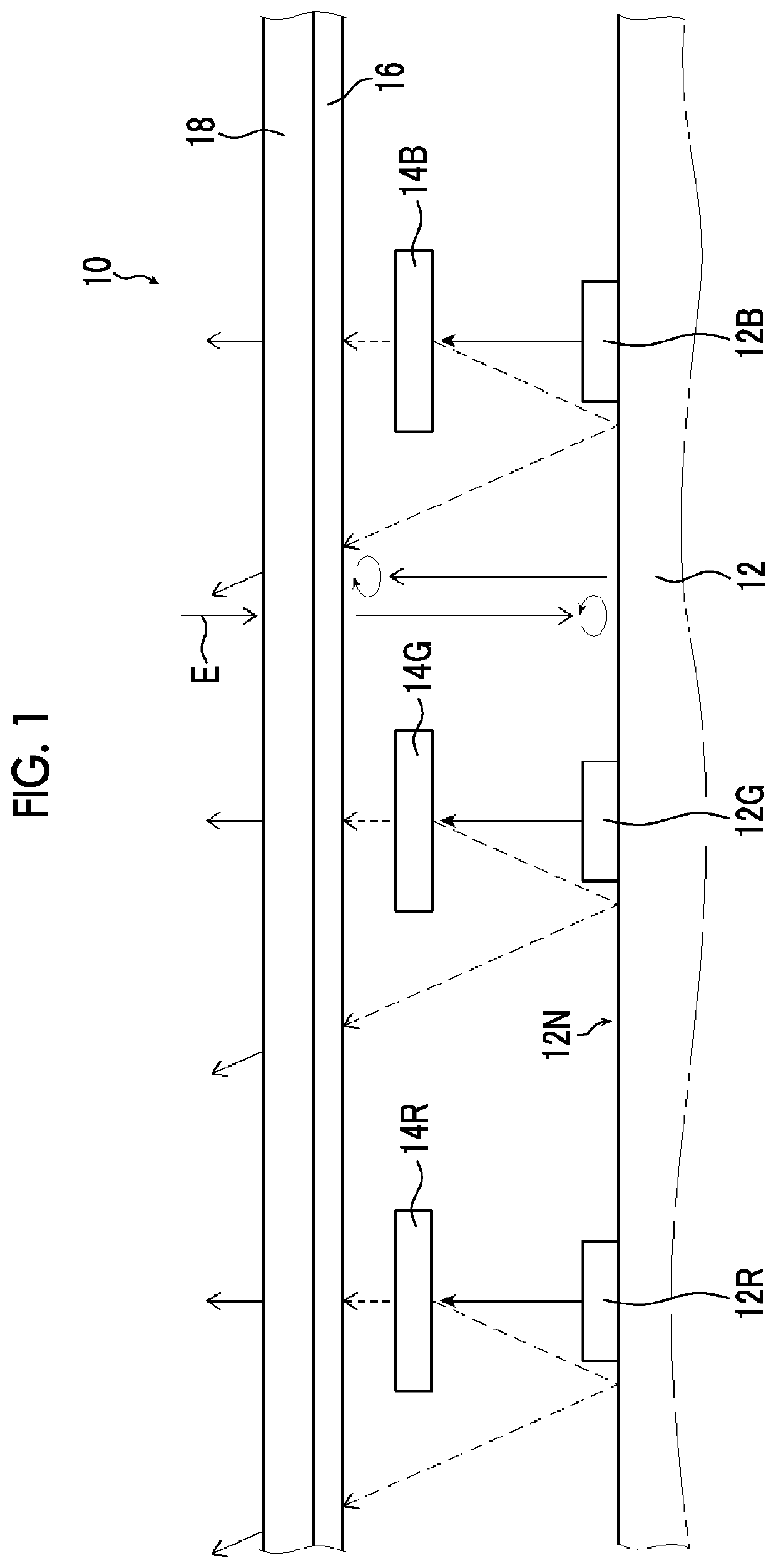
[0297]A commercially available organic EL display device (manufactured by SAMSUNG, SC-04E) including an R light emitting portion (red organic electroluminescent layer), a G light emitting portion (green organic electroluminescent layer), and a B light emitting portion (blue organic electroluminescent layer) was prepared.

[0298]From this organic EL display device, a polarizing plate and an optical film were removed, and the surface of a barrier layer protecting a light emitting element was exposed. The substance obtained in this way was used as an organic EL substrate.

[0299]In this organic EL substrate, the R light emitting portion has an emission spectrum with a central wavelength of 650 nm and an emission bandwidth of 50 nm, the G light emitting portion has an emission spectrum with a central wavelength of 550 nm and an emission bandwidth of 45 nm, and the B light emitting portion has an emission spectrum with a central wavelength of 450 nm and an emission bandwidth of 40 nm.

[...

example 2

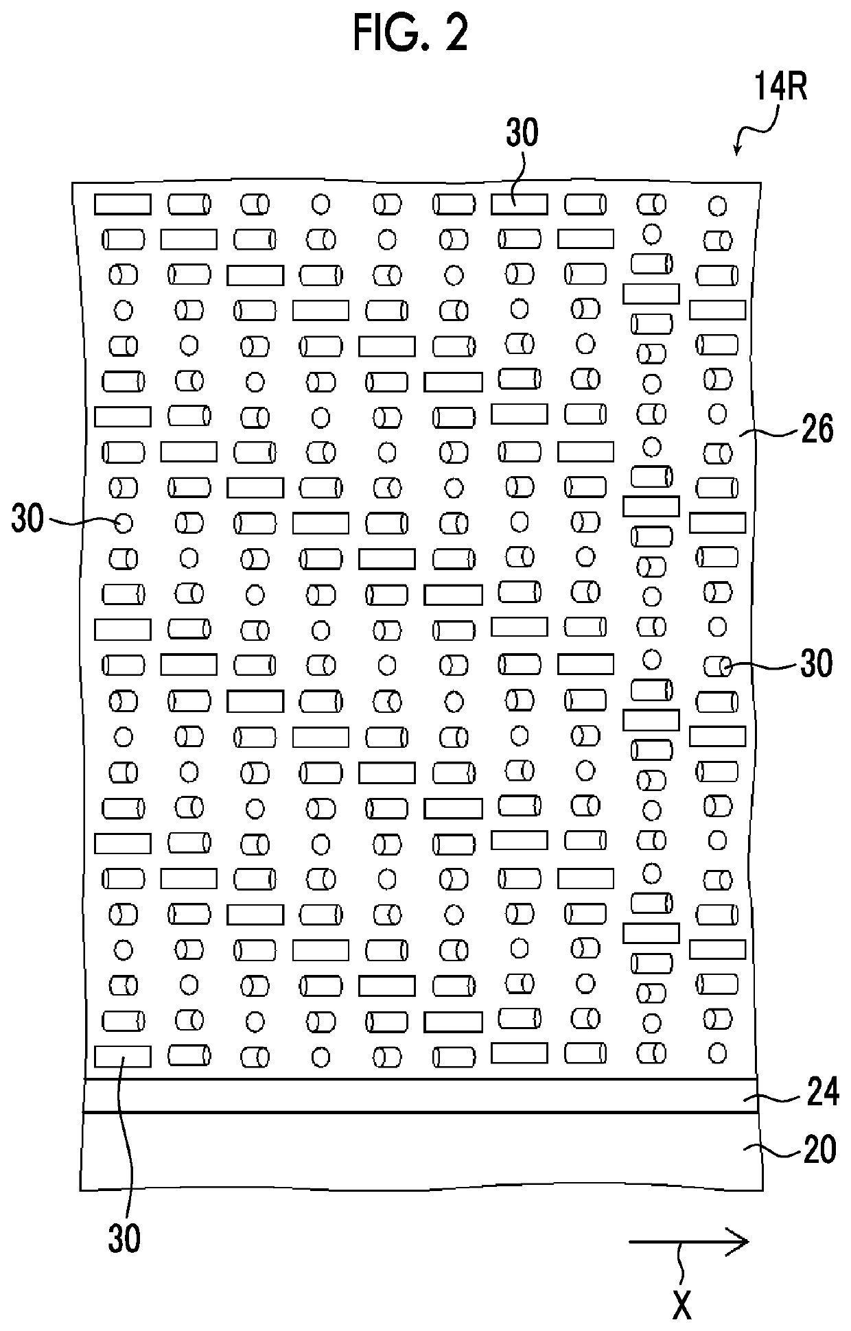
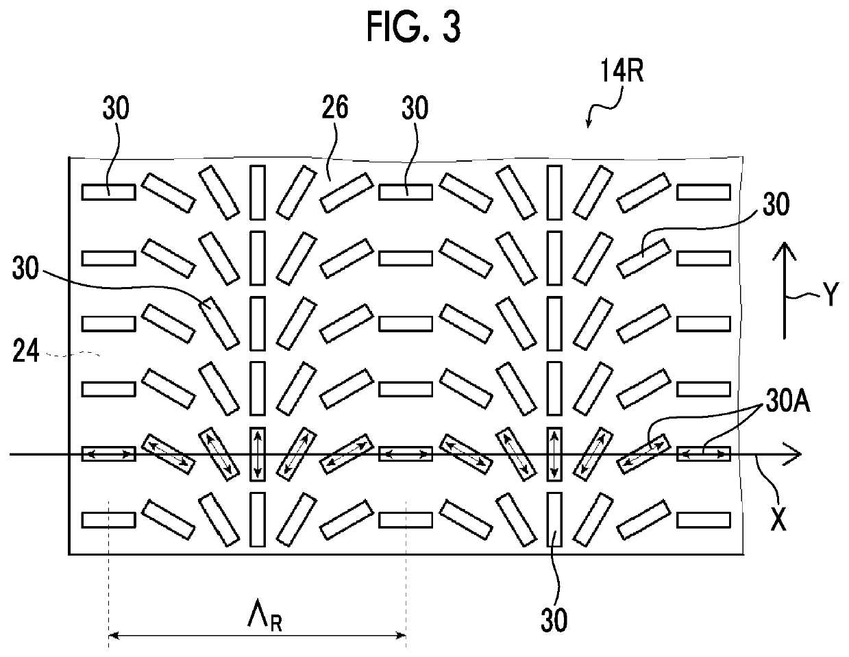
[0337]For performing exposure by using the exposure device shown in FIG. 6 so as to form an alignment film for forming a circularly polarized light-separating layer, first, an alignment film was exposed through a mask in which only a region corresponding to an R light emitting portion of an organic EL substrate is a light transmission portion and other regions are light shielding portions.

[0338]Then, the intersecting angle α of two light rays MA and MB was changed, and the alignment film was exposed through a mask in which only a region corresponding to a G light emitting portion of the organic EL substrate is a light transmission portion and other regions are light shielding portions.

[0339]Thereafter, the intersecting angle α of two light rays MA and MB was changed, and the alignment film was exposed through a mask in which only a region corresponding to a B light emitting portion of the organic EL substrate is a light transmission portion and other regions are light shielding port...

example 3

[0344]An alignment film was exposed in the same manner as in Example 2, thereby forming an alignment film for forming a circularly polarized light-separating layer.

[0345]The alignment film was coated with the liquid crystal compositions LC-R, LC-G, and LC-B in the same manner as in Example 1.

[0346]Thereafter, the liquid crystal composition LC-1 was allowed to age by being heated at a film surface temperature of 95° C. for 60 seconds and then immediately exposed through the mask conceptually shown in FIG. 11 in the air at 25° C. by using an ultrahigh-pressure mercury lamp (manufactured by Canon Inc., PLA-501F exposure machine) at an exposure amount of 100 mJ / cm2.

[0347]In the mask shown in FIG. 11, the portion of the gridded region A is a light shielding portion, and other regions R, G, and B are light transmission portions. In terms of position, the regions R, G, and B correspond to the R light emitting portion, the G light emitting portion, and the B light emitting portion of the or...


PUM


Abstract

An object of the present invention is to provide an optical device that can accomplish both the effect of preventing external light reflection and the improvement of utilization efficiency of light emitted from an organic electroluminescent element. The object is achieved by an optical device having an organic electroluminescent substrate, a circularly polarized light-separating layer separating light into right-handed circularly polarized light and left-handed circularly polarized light, a λ / 4 plate, and a polarizer, wherein the circularly polarized light-separating layer has a liquid crystal alignment pattern in which a liquid crystal compound is twisted and aligned along a helical axis extending in a thickness direction and the direction of an optical axis derived from the liquid crystal compound changes while continuously rotating in one direction in the plane.

Description

CROSS-REFERENCE TO RELATED APPLICATIONS[0001]This application is a Continuation of PCT International Application No. PCT / JP2019 / 008685 filed on Mar. 5, 2019, which claims priority under 35 U.S.C. § 119(a) to Japanese Patent Application No. 2018-039651 filed on Mar. 6, 2018. The above application is hereby expressly incorporated by reference, in its entirety, into the present application.BACKGROUND OF THE INVENTION1. Field of the Invention[0002]The present invention relates to an optical device using organic electroluminescence.2. Description of the Related Art[0003]In recent years, as a display device replacing a liquid crystal display device, organic electroluminescence (organic electro luminescence (EL) (organic light emitting diode (OLED)) has been developed continuously, and a 60-inch large display device (display) has started appearing.[0004]The surface of the organic EL substrate constituting the organic EL display device has a high reflectance. Accordingly, particularly in a ...

Claims


Application Information

Patent Timeline
IPC IPC(8): H01L51/52G02B27/28G02B5/30H01L27/32
CPCH01L51/5281G02B27/283G02B5/3016H01L27/3232H05B33/12B32B7/023H05B33/02G02B27/286H10K59/8791H10K50/86H10K59/50
Inventor SAITOH, YUKITOSATO, HIROSHI
Owner FUJIFILM CORP
Why Eureka
Try Eureka