Manufacturing method of light emitting diode chips and light conversion device

A light-emitting diode and chip technology, applied in laser welding equipment, manufacturing tools, welding equipment, etc., can solve the problems of low yield rate of LED chips, achieve the effect of improving external quantum efficiency, increasing yield rate, and avoiding chip breakage

Active Publication Date: 2017-10-27
HC SEMITEK ZHEJIANG CO LTD
View PDF5 Cites 0 Cited by
  • Summary
  • Abstract
  • Description
  • Claims
  • Application Information

AI Technical Summary

Problems solved by technology

[0006] In order to solve the problem of low yield rate of LED chips in the prior art, an embodiment of the present invention provides a method for preparing a light emitting diode chip and a light conversion device

Method used


Image

  • Manufacturing method of light emitting diode chips and light conversion device
  • Manufacturing method of light emitting diode chips and light conversion device
  • Manufacturing method of light emitting diode chips and light conversion device

Examples


Embodiment 1

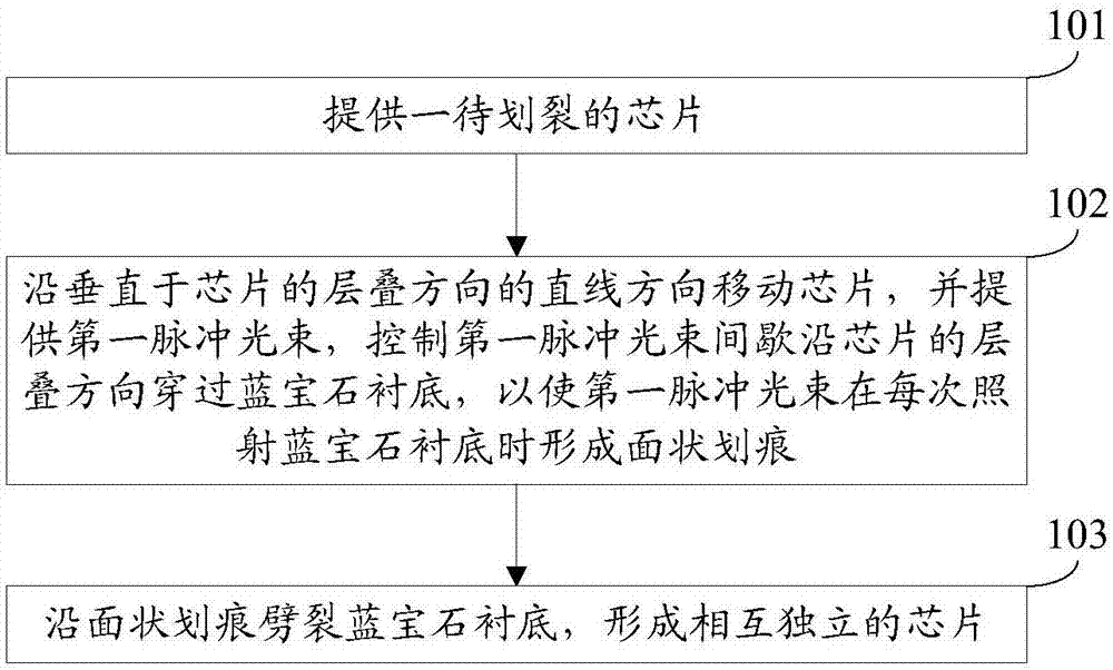
[0041] The embodiment of the present invention provides a method for preparing a light-emitting diode chip, see figure 1 , the preparation method comprises:

[0042] Step 101: Provide a chip to be diced.

[0043] In this embodiment, the chip includes a sapphire substrate and an N-type semiconductor layer, a light-emitting layer, a P-type semiconductor layer, a current blocking layer, a transparent conductive layer, and a P-type electrode stacked sequentially on the sapphire substrate. A groove extending from the P-type semiconductor layer to the N-type semiconductor layer along the stacking direction of the chip is opened, and an N-type electrode is arranged on the N-type semiconductor layer in the groove.

[0044] Specifically, this step 101 may include:

[0045] In the first step, an N-type semiconductor layer, a light-emitting layer, and a P-type semiconductor layer are sequentially grown on a sapphire substrate.

[0046]In the second step, a groove extending from the P-...

Embodiment 2

[0089] An embodiment of the present invention provides a light conversion device used in the preparation method provided in Embodiment 1, see Figure 5 , the device consists of:

[0090] a laser 201, configured to emit a second pulse beam;

[0091] The lens group 202 is used to diverge the second pulsed beam emitted by the laser 201 into a third pulsed beam, and the cross-sections of the second pulsed beam and the third pulsed beam parallel to the surface of the sapphire substrate provided with the N-type semiconductor layer are both A circle with a constant area, and the cross-sectional area of ​​the second pulsed beam is smaller than the cross-sectional area of ​​the third pulsed beam;

[0092]The filter plate 203 is used to intercept the third pulse beam formed by the lens group 202 into a fourth pulse beam, and the cross section of the fourth pulse beam parallel to the surface of the sapphire substrate provided with the N-type semiconductor layer has a constant area rect...


PUM

PropertyMeasurementUnit
lengthaaaaaaaaaa
lengthaaaaaaaaaa

Abstract

The invention discloses a manufacturing method of light emitting diode chips and a light conversion device, and belongs to the technical field of semiconductors. The method comprises the steps of: providing a chip to be split; moving the chip along the linear direction perpendicular to the laminating direction of the chip, providing a first pulse beam, and controlling the first pulse beam to penetrate through a sapphire substrate along the laminating direction of the chip, so that the first pulse beam forms a planar scratch when irradiating the sapphire substrate every time, the area of the cross section, parallel to the surface, provided with an N-type semiconductor layer, of the sapphire substrate, of the first pulse beam is reduced and then increased along the irradiation direction of the first pulse beam, the cross section is a line segment parallel to the linear direction when the area is minimum, and the length of the line segment is greater than the moving distance of the chip between two adjacent times when the first pulse beam irradiates the sapphire substrate; and splitting the sapphire substrate along the planar scratch to form independent chips. The method improves the yield of the chips.

Description

technical field [0001] The invention relates to the technical field of semiconductors, in particular to a method for preparing a light-emitting diode chip and a light conversion device. Background technique [0002] Light Emitting Diode (English: Light Emitting Diode, referred to as: LED) is a new generation of solid-state lighting source with high efficiency, environmental protection and green. It has the advantages of low voltage, low power consumption, small size, light weight, long life and high reliability. It is used in traffic signal lights, car interior and exterior lights, urban landscape lighting, mobile phone backlight, outdoor full-color display screens and other fields. [0003] The chip is the most important part of the LED. The current chip preparation method includes: first forming an N-type semiconductor layer, a light-emitting layer, a P-type semiconductor layer, a current blocking layer, a transparent conductive layer, a P-type electrode and an N-type semi...

Claims


Application Information

Patent Timeline
Patent Type & Authority Applications(China)
IPC IPC(8): H01L33/00B23K26/073
CPCB23K26/0738H01L33/007
Inventor 兰叶顾小云黄龙杰杨春艳吴志浩王江波
Owner HC SEMITEK ZHEJIANG CO LTD
Why Eureka
Try Eureka