Light-emitting thyristor, light-emitting thyristor array, exposure head, and image forming apparatus

Active Publication Date: 2020-09-10
CANON KK
View PDF0 Cites 0 Cited by
  • Summary
  • Abstract
  • Description
  • Claims
  • Application Information

AI Technical Summary

Benefits of technology

The invention is about a light-emitting thyristor that can improve its light emission efficiency while still performing its thyristor function.

Problems solved by technology

S63-196084, however, it is difficult to improve light emission efficiency while maintaining a function as a thyristor.

Method used


Image

  • Light-emitting thyristor, light-emitting thyristor array, exposure head, and image forming apparatus
  • Light-emitting thyristor, light-emitting thyristor array, exposure head, and image forming apparatus
  • Light-emitting thyristor, light-emitting thyristor array, exposure head, and image forming apparatus

Examples


first example

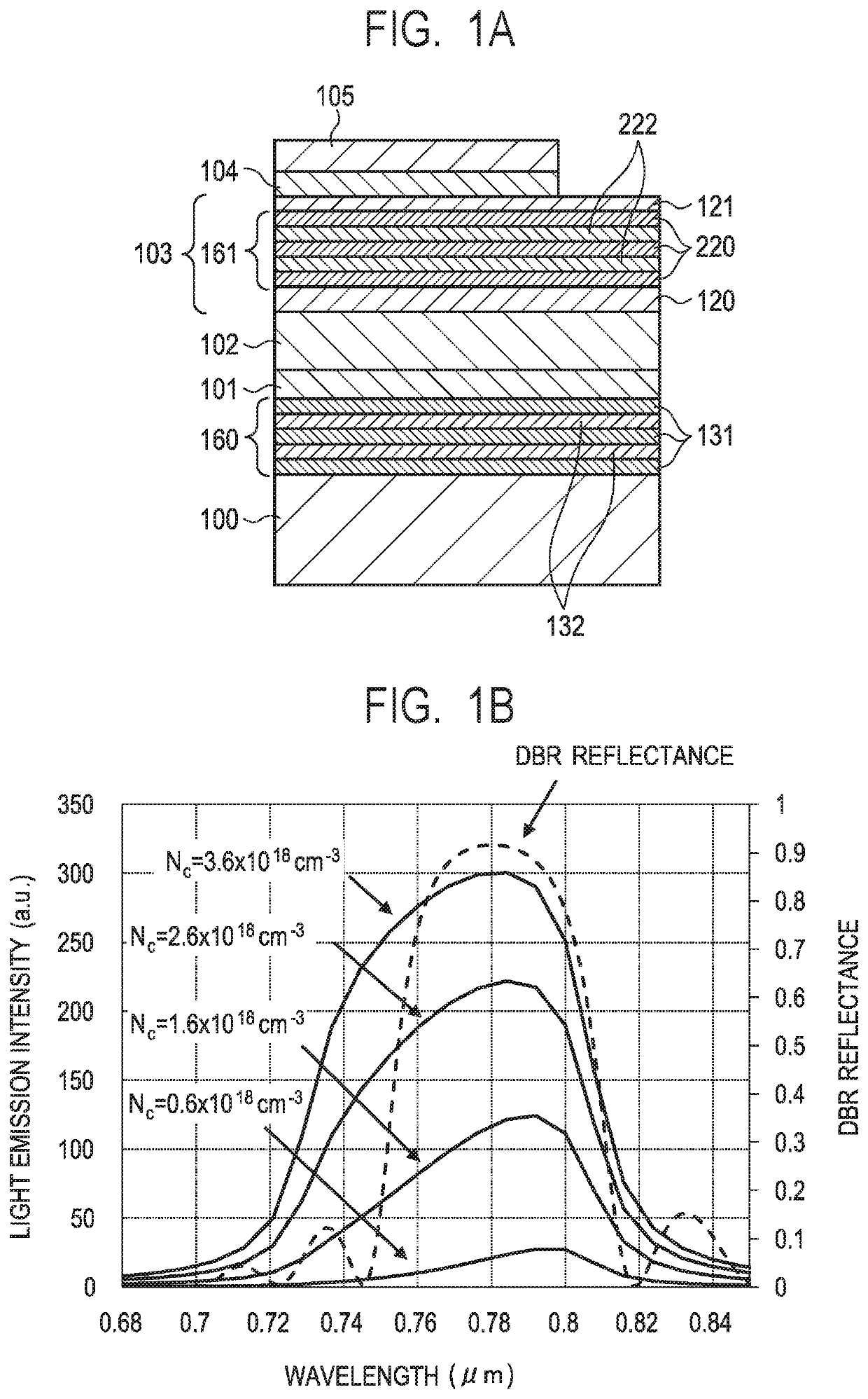
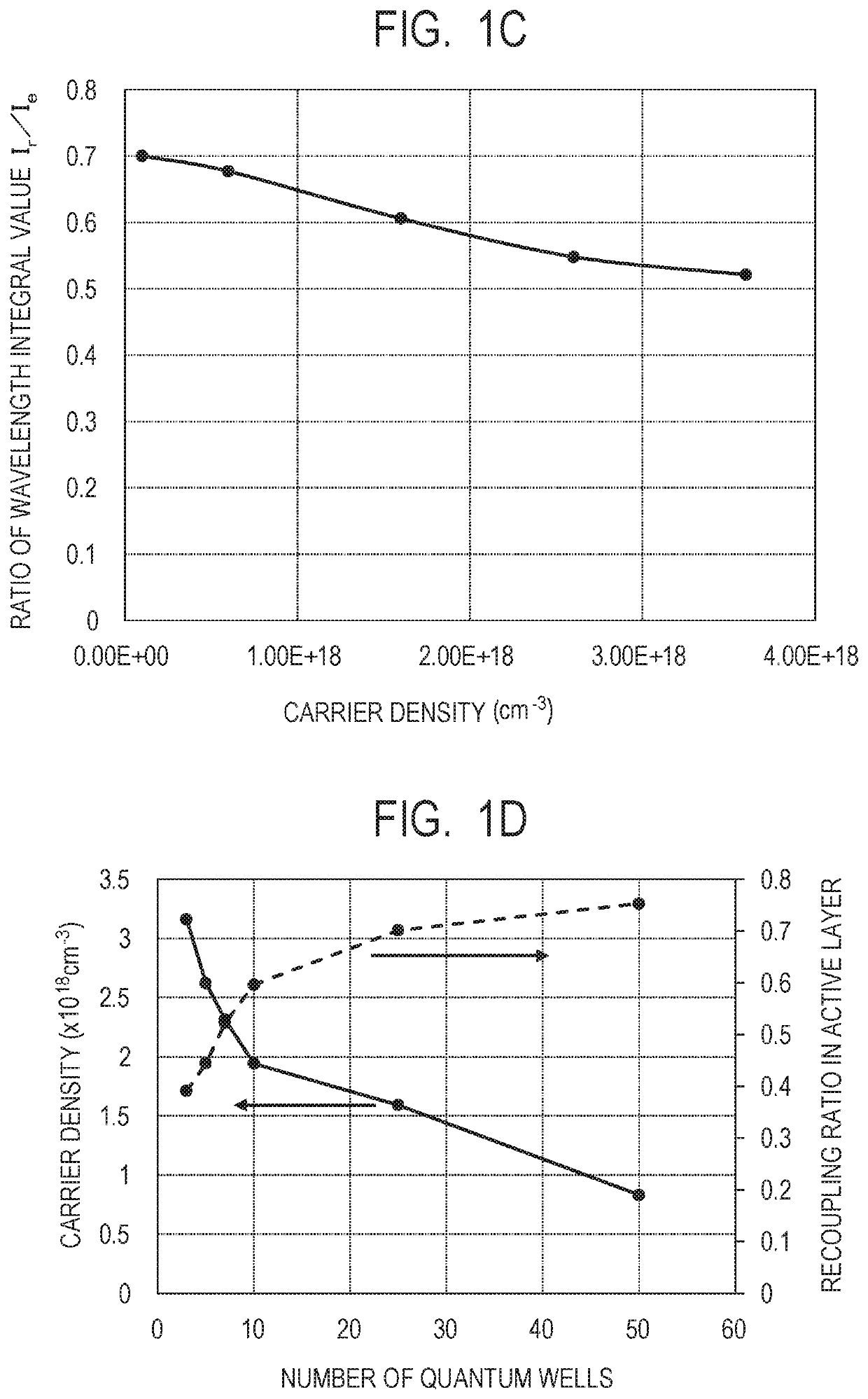
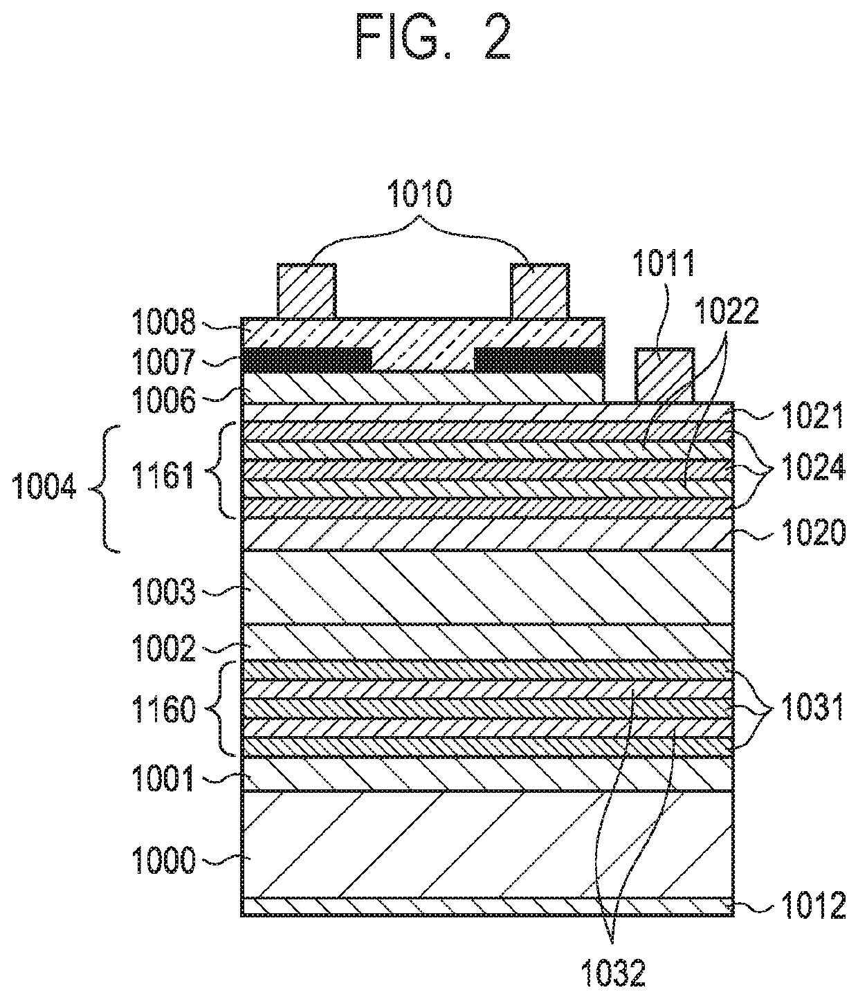
[0055]FIG. 2 is an element sectional view of a light-emitting thyristor of a first example. In the light-emitting thyristor of the present example, an n-type GaAs buffer layer 1001, a semiconductor DBR layer 1160, a cathode layer 1002, a p-base layer 1003, an n-gate layer 1004, and an anode layer 1006 are stacked in this order on an n-type GaAs substrate 1000. A current constriction portion 1007 in which an electrical opening (a region in which a conductivity is higher than the outer circumference portion of the opening) is partially provided is formed on the anode layer 1006. A transparent conductive layer 1008 that is transparent to a light emission wavelength is formed on the current constriction portion 1007. An anode electrode 1010 is formed on the transparent conductive layer 1008. The anode electrode 1010 is a ring electrode (flame-shape electrode) and is structured to extract a light emitted by the n-gate layer 1004 and the p-base layer 1003. Further, a gate electrode 1011 i...

second example

[0060]FIG. 3 is an element sectional view of a light-emitting thyristor of a second example. In the light-emitting thyristor of the present example, an n-type GaAs buffer layer 2001, a semiconductor DBR layer 2160, a cathode layer 2002, a p-base layer 2003, an n-gate layer 2004, and an anode layer 2006 are stacked in this order on an n-type GaAs substrate 2000. A current constriction portion 2007 in which an electrical opening (a region in which a conductivity is higher than the outer circumference portion of the opening) is partially provided is formed on the anode layer 2006. A transparent conductive layer 2008 that is transparent to a light emission wavelength is formed on the current constriction portion 2007. An anode electrode 2010 is formed on the transparent conductive layer 2008. The anode electrode 2010 is a ring electrode (flame-shape electrode) and is structured to extract a light emitted by the n-gate layer 2004 and the p-base layer 2003. Further, a gate electrode 2011 ...

third example

[0077]FIG. 4 is an element sectional view of a light-emitting thyristor of a third example. Note that, since the configuration of the present example is similar to the configuration of the second example, the same members as those of the second example are labeled with the same references, and the description thereof will be omitted or simplified in the present example.

[0078]In the light-emitting thyristor of the present example, the n-type GaAs buffer layer 2001, the semiconductor DBR layer 2160, the cathode layer 2002, the p-base layer 2003, the n-gate layer 2004, and the anode layer 2006 are stacked in this order on the n-type GaAs substrate 2000. Further, the anode electrode 2010 is formed on the anode layer 2006 via the current constriction portion 2007 and the transparent conductive layer 2008. The anode electrode 2010 is a ring electrode (flame-shape electrode) and is structured to extract a light emitted by the n-gate layer 2004 and the p-base layer 2003. Further, the gate e...


PUM


Abstract

A light-emitting thyristor includes a layered structure having a semiconductor DBR layer, a first semiconductor layer of a first conductivity type, a second semiconductor layer of a second conductive type, a third semiconductor layer, and a fourth semiconductor layer of the second conductivity type in this order on a semiconductor substrate, the third semiconductor layer has at least one fifth semiconductor layer of the first conductivity type and a multi-quantum well structure, the fifth semiconductor layer is present between the second semiconductor layer and the multi-quantum well structure, the multi-quantum well structure is formed of barrier layers and quantum well layers, and the number of the quantum well layers is greater than or equal to 10.

Description

BACKGROUND OF THE INVENTIONField of the Invention[0001]The present invention relates to a light-emitting thyristor, a light-emitting thyristor array, an exposure head, and an image forming apparatus.Description of the Related Art[0002]As a head used for forming a latent image on a photosensitive drum of an image forming apparatus, a surface light-emitting element array is used. In a typical configuration of such a head, a plurality of plane light-emitting elements (light-emitting elements that emit light perpendicular to the primary face of a semiconductor substrate) are aligned in a certain direction, and a lens array is arranged in the same direction as the alignment direction of light-emitting elements. The light from the light-emitting elements are then captured on the photosensitive drum through the lens. As the light-emitting element, an element formed of a light-emitting diode (LED) and an element formed of a light-emitting thyristor are known.[0003]The configuration disclose...

Claims


Application Information

Patent Timeline
IPC IPC(8): H01L33/00H01L33/06H01L33/30H01L27/15G03G15/04
CPCH01L33/0016H01L33/06G03G15/04036H01L33/30H01L27/153H01L33/10G03G15/04045H01L33/46
Inventor UCHIDA, TAKESHISUGA, TAKAKO
Owner CANON KK
Why Eureka
Try Eureka