Infrared sensor and infrared sensor array

a technology of infrared sensors and arrays, applied in the field of infrared sensors, can solve the problems of difficult to precisely detect the temperature of semiconductor substrates, and achieve the effect of small offset and large s/n ratio without complicating circuit configuration

Active Publication Date: 2008-02-19
PANASONIC CORP
View PDF19 Cites 53 Cited by
  • Summary
  • Abstract
  • Description
  • Claims
  • Application Information

AI Technical Summary

Benefits of technology

[0034]With the infrared sensor of the present invention, it is possible to realize an infrared sensor and an infrared sensor array in which it is not necessary to correct a temperature change of the semiconductor substrate, and to realize an infrared sensor and an infrared sensor array capable of obtaining a signal with a small offset and a large S / N ratio without complicating the circuit configuration.

Problems solved by technology

Thus, while it is necessary to accurately measure the temperature of the semiconductor substrate in order to correct a variation of the resistance value of the dummy resistor 152, it is not easy to precisely detect the temperature of the semiconductor substrate.
Therefore, even if there is no infrared light incident on the sensor, there occurs an offset, being a spurious signal output.

Method used


Image

  • Infrared sensor and infrared sensor array
  • Infrared sensor and infrared sensor array
  • Infrared sensor and infrared sensor array

Examples


first embodiment

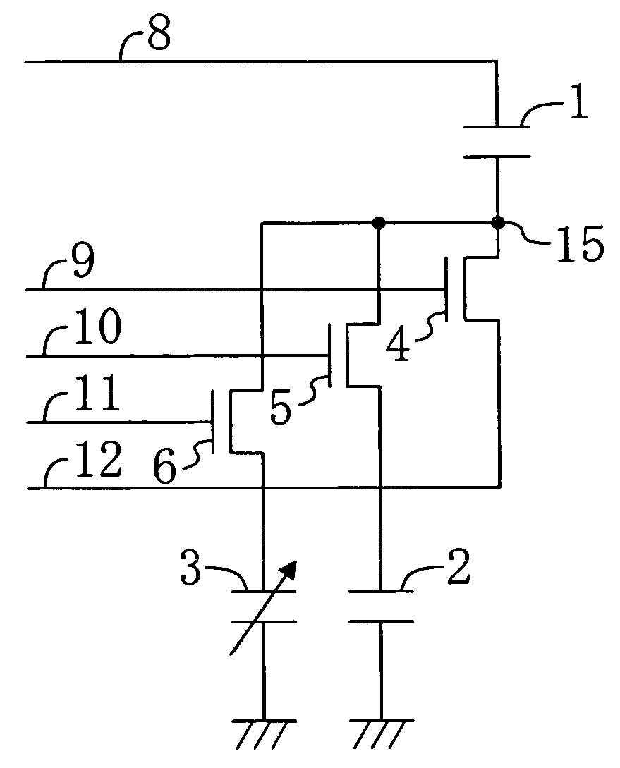
[0121]An infrared sensor according to a first embodiment of the present invention will now be described with reference to the drawings. FIG. 1 is a basic circuit diagram showing an infrared sensor of the present embodiment.

[0122]As shown in FIG. 1, in the infrared sensor of the present embodiment, a first terminal of a series capacitor element 1 is electrically connected to first terminals of a reference capacitor element 2 and an infrared-detecting capacitor element 3 via a reference capacitor element control switch 5 and an infrared-detecting capacitor element control switch 6, each being a MOS transistor, thus forming an output node 15. The capacitance value of the series capacitor element 1 and that of the reference capacitor element 2 are set so as to be substantially the same as the capacitance value of the infrared-detecting capacitor element 3 when there is no incident infrared light. Thus, these capacitance values are equal to one another within the range of their tolerance...

second embodiment

[0133]A second embodiment of the present invention will now be described with reference to the drawings. FIG. 3 is a basic circuit diagram showing an infrared sensor array of the present embodiment.

[0134]In the present embodiment, four infrared sensors, i.e., an infrared sensor 20, an infrared sensor 21, an infrared sensor 22 and an infrared sensor 23, are arranged in a matrix pattern to form an infrared sensor array, as shown in FIG. 3. The basic configuration of each infrared sensor is the same as that of the first embodiment.

[0135]The bias control lines 9, the reference capacitor element control lines 10 and the infrared-detecting capacitor element control lines 11 of the infrared sensors 20 to 23 are commonly connected to a vertical scanning and signal controlling section 28. The bias lines 12 are all connected in parallel and are connected to a bias power supply 37. The power supply lines 8 are commonly connected to the vertical scanning and signal controlling section 28 via po...

third embodiment

[0147]A third embodiment of the present invention will now be described with reference to the drawings. FIG. 5 shows a basic circuit configuration of an infrared sensor of the present embodiment. As shown in FIG. 5, the infrared sensor of the present embodiment includes an output circuit 90, being an impedance conversion circuit or an amplifier circuit, provided downstream of the output node 15 shown in the first embodiment.

[0148]FIG. 6 shows a source follower circuit as an example of the output circuit 90. As shown in FIG. 6, the source follower circuit includes an MOS transistor 91 and an MOS transistor 92 connected in series with each other between the power supply and the ground. The signal from the output node 15 is input to the gate of the transistor 91, and a bias voltage is applied to the gate of the transistor 92. With such a configuration, an impedance-converted signal is output to a source follower output node 93, being the node between the transistor 91 and the transisto...


PUM


Abstract

An infrared sensor includes a series capacitor element and a reference capacitor element each exhibiting a predetermined capacitance value; an infrared-detecting capacitor element whose capacitance value varies depending on an intensity of infrared light incident on the element; and an output node being a node at which a first terminal of the series capacitor element, a first terminal of the reference capacitor element and a first terminal of the infrared-detecting capacitor element are connected to one another. The intensity of infrared light is output as a potential difference between the reference potential which is brought to a potential by applying a predetermined voltage between the series capacitor element and the reference capacitor element and the detection potential which is brought to a potential by applying a predetermined voltage between the series capacitor element and the infrared-detecting capacitor element.

Description

[0001]This application is the U.S. National Phase under 35 U.S.C. § 371 of International Application No. PCT / JP05 / 017070, filed Sep. 15, 2005, which in turn claims the benefit of Japanese Application No. 2004-303262, filed Oct. 18, 2004, the disclosures of which Applications are incorporated by reference herein in their entirety.TECHNICAL FIELD[0002]The present invention relates to an infrared sensor for detecting infrared light being radiated from an object or a human body.BACKGROUND ART[0003]An infrared sensor can detect infrared light being radiated from an object such as a human body. With the ability for non-contact detection of the existence or the temperature of an object, it is expected to find applications in a variety of fields of technology. Particularly, an infrared sensor array including a plurality of infrared sensors arranged in a matrix pattern is capable of obtaining a two-dimensional infrared light image, and is expected to find applications in an even wider variet...

Claims


Application Information

Patent Timeline
Patent Type & Authority Patents(United States)
IPC IPC(8): G01J5/00
CPCG01J1/46G01J5/24H04N5/33
Inventor MURATA, TAKAHIKOYAMAGUCHI, TAKUMIKASUGA, SHIGETAKAYOSHIDA, SHINJIIKEDA, YOSHITO
Owner PANASONIC CORP
Why Eureka
Try Eureka